 |
How to Design a Class-E Transmitter for Your LowFER Beacon
by
Bill Cantrell “TEXAS” & WD5CVG
Aug `98
Converted to HTML (with permission) by K3PGP - rev 0.3a
We certainly need all of the output power that we can get. FCC Part 15 allows us only one watt of input power into our transmitter. If we have a 100% efficient transmitter, then we get the full one-watt of power out for the antenna. The Class-E design is a perfect choice for the LowFER or MedFER experimenter due to its simplicity and high efficiency (essentially ~100%). With no transformers, no push-pull, and only one switching transistor, it has fewer parts than the more common Class-D transmitter. So it is easier to build, but it is also more efficient than Class-D. The Class-E topology has been described previously in [1].
The purpose of this article is four-fold:
(1) explain how the class-E circuit works
(2) present the actual design equations in a ‘cookbook
recipe’ form
(3) modify the Class-E circuit to make it easier to peak-tune
(4) provide computer simulation results using PSPICE [2].
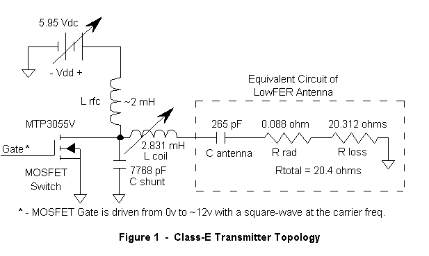
Refer to Figure 1:
|
This is a simplified schematic of the Class-E transmitter stage used in the TEXAS Beacon. (The gate driving circuitry is not shown here but will be the subject of next month’s article.) This is an incredibly simple circuit: one MOSFET switch, a silvered- mica shunt cap, one torroidal rf-choke (Lrfc), and a large Hi-Q air-wound coil (Lcoil). For the coil, I use a Bill Bowers special [3,4]. A few of the turns are part of an adjustable rotating-link for fine-tuning the beacon to exact resonance. The coil’s Q is > 500. There is an adjustable DC supply (Vdd) that serves as the fine-adjustment for obtaining exactly 1.0 watt input power. I use a Motorola LM317T 3-terminal regulator to perform this function. The circuitry shown in the dashed-box in Fig. 1 is an equivalent circuit of the beacon antenna structure. A technique has been described in [5] for determining the parameters shown. Note that the DC supply voltage appears on the beacon antenna structure. This should not be a problem, but if you don’t like a few volts dc on your tower, just add a large (>10 x Cant) hi-Q dc blocking cap in series with Lcoil.
How the Class-E Circuit Works
It is standard practice to make a few simplifying assumptions when analyzing switch- mode power supplies. The Class-E transmitter can actually be thought of as a resonant-mode switching power supply. It takes DC input power and produces an AC sine-wave output at the carrier frequency. We assume that the DC feed choke (Lrfc) is large so that the DC input current through it is essentially constant. This is true once periodic steady-state is reached. We also assume that the Q of the series-resonant output circuit is very high (Q=160 for TEXAS). This causes the AC current feeding the antenna to be a pure sine-wave with no harmonic content. Third, we assume that the MOSFET switching transistor can be modeled as a perfect switch. That is to say, it is either ON with zero voltage across it, or it is OFF with zero current through it. Either way, the power dissipation in the switch is essentially zero, except during the very fast switching intervals that occur twice per carrier cycle. Note that the drain-to-source capacitance of the MOSFET can be absorbed into the shunt capacitor (Cshunt) during the design phase. This is a big advantage for the Class-E circuit over the Class-D design [6]. The switch’s capacitance does not work against us.
Using these assumptions, we can write design equations to describe circuit behavior. There are several solutions to the equations, but we would like the one solution that offers the highest efficiency and lowest sensitivity to part value variation. This imposes a few more constraints on our choice of component values. Up to this point we were free to choose the duty-cycle of our MOSFET switch. It could be something other than 50% if desired. But for maximum efficiency, we need a square-wave with equal ON and OFF times to drive the gate of the MOSFET. This much is intuitive, but the rest of Class-E operation is not so obvious. Figures 2(a) and 2(b) are shown to help clarify circuit operation:
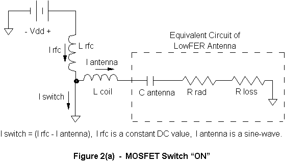 |
In Fig. 2(a) the MOSFET switch is ON. The voltage across Cshunt is zero so no current flows in the capacitor. It can be removed from the equivalent circuit. In periodic steady- state the DC current is always constant regardless of what the MOSFET switch is doing, and so is the peak AC output current flowing to the load (antenna). By Kirchoff’s current law (KCL) the difference between these two currents is the MOSFET switch current.
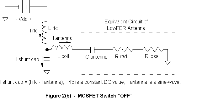 |
In Fig. 2(b) the MOSFET switch is now OFF and can be removed from the diagram. The voltage across Cshunt is no longer zero and current will flow in the capacitor. Again, the DC current in Lrfc is always constant, so now the capacitor current in Cshunt will be the difference between the current in Lrfc and the load current, due to KCL. A simultaneous solution of the circuit equations has been performed [7,8,9,10]. The critical factor is the voltage across Cshunt when the MOSFET switch turns ON again. If any charge is left on this capacitor, the switch will quickly discharge it and power will be wasted. Therefore we want the capacitor voltage to just reach zero when the switch turns on again. Optimum efficiency imposes the further constraint on Cshunt that the first derivative of the capacitor voltage is also zero at the moment the switch turns ON, i.e., the slope should be zero. To put it another way, the waveform comes in for a “soft landing”. This is illustrated in Figures 3(a) through 3(d):
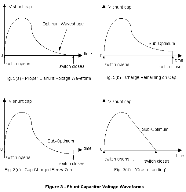 |
In Fig. 3(a) the cap voltage and its derivative are both zero. This is optimum. In Figs. 3(b) and 3(c), the derivative is zero, but now there is either a positive or a negative voltage residual on the cap when the switch closes. In this situation, the switch conducts and a large current spike discharges the capacitor to zero through the switch. This is definitely not optimum. In Fig. 3(d) the voltage on the cap is zero when the switch closes, but there is a current flowing in the shunt cap. This current will immediately begin to flow through the switch when it closes. Because Ic = C x (dVc / dt), the current in the capacitor will be zero if the slope is zero. If the switch voltage and the switch current are zero when the switch closes, no power will be wasted during the switch-ON transition time. At this point you might be wondering “Why have a switch at all? It doesn’t seem to be doing much.” Here is a description of what is happening in periodic steady-state:
Let’s start with the MOSFET switch closing. Lrfc is shorted to ground, so current builds in it very slightly (for this is a large inductance) and its magnetic field grows as it stores a bit more energy. This dc current flows through the switch to ground. AC current is flowing out to the antenna, for it is in its positive portion of the sine-wave cycle at this moment. However, the sine-wave current begins to drop through zero and reverses itself, while the switch is still closed. Now, AC current returns from the antenna as the switch opens abruptly. The current that was flowing in the switch must go somewhere, so instantaneously, it flows through the shunt capacitor. This starts a positive voltage building up on the capacitor as it stores energy in the form of an electric field. See Figure 4 for a PSPICE plot of these currents. At this point, the negative antenna current is beginning to drop to zero and reverse itself again. It will go positive because the hi-Q series resonant circuit formed by C ant and Lcoil forces a sine-wave current to flow back and forth in the output circuit. The voltage on Cshunt increases and peaks during this time. However, as the antenna current increases in the positive direction, energy is transferred from the shunt cap to the output circuit. The trick is to choose the component values so that the shunt cap is drained to zero just as the switch closes again. Note in Fig. 4 if you piece the two discontinuous current segments together, e.g., the switch current and the shunt cap current, you get a sine-wave current that is out of phase with the antenna current and is offset by the DC input current level. This must be the case due to KCL as described earlier.
In simple terms, the switch causes current to flow in Lrfc. The inductance of Lrfc forces current to flow in Cshunt when the switch opens, which transfers energy from Lrfc to Cshunt. Cshunt then transfers all of its energy to the output circuit during each cycle. The switch regulates the entire process to keep the frequency exact. No energy is wasted when the switch closes again because the closing coincides with zero voltage on the cap and zero current through cap.
Class-E Design Equations
Okay, enough already. . . How do I design it? Here’s the procedure. For now we will assume 100% efficiency using Equation (1):
(Vload rms) is the rms voltage across the series combination of Rloss and Rrad. You need to know your antenna capacitance (C ant) and your antenna resistance (Rloss + Rrad) in order to get started. Rloss includes any loading coil losses. As mentioned earlier, refer to [5] for an idea of how to measure this for an existing beacon station. Otherwise, you can estimate it empirically using [11], and tweak the values later by using an oscilloscope to look at the voltage waveforms. Most installations have a loss resistance somewhere between 100 ohms (poor) to 50 ohms (fair) to 10 ohms (excellent). Antenna capacitance is a function of top-hat size and tower height. This can be anywhere around 120 to 500 pF, the more the better [12]. If you can’t measure it directly, take your best guess. Most installations require a few iterations to obtain optimum performance. A class-E transmitter may require a little extra effort to get the better efficiency that it provides.
We will use TEXAS as a design example, C ant = 265 pF, (Rloss + Rrad) = 20.4 ohms, and fo = 184.400 kHz. From Eqn. (1) Vload rms = 4.516 Vrms. We compute the required supply voltage (Vdd) by using Equation (2):
Therefore Vdd = 5.947 Vdc. Note that this input voltage is not a free parameter to choose. This voltage determines the power supplied to the antenna. (It can be tweaked to adjust the input power to exactly one watt.) We use Eqn. (1) again to determine the DC supply current. Since Vdd = 5.947 Vdc, the DC supply current (Irfc) will be 168.1 mA dc. Similarly, the AC antenna current (I antenna) will be 221.4 mA rms. Simple, eh? The next step is to compute Cshunt using Equation (3):

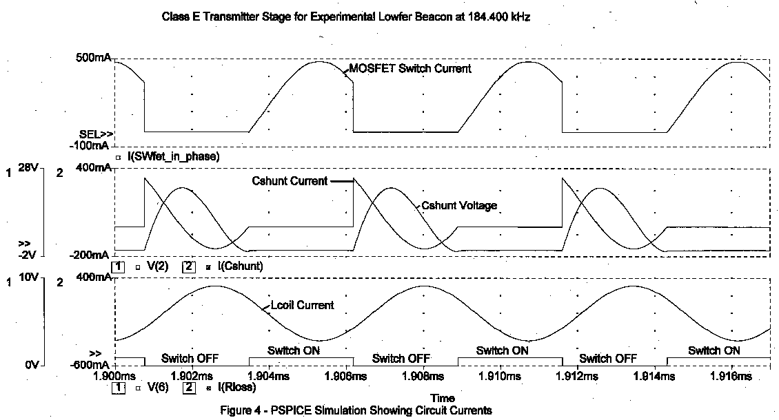 |
The drain to source capacitance (Cds) of the Motorola MTP3055V MOSFET switch is ~200 pF, so this will be subtracted from the actual value calculated. Therefore Cshunt is calculated to be 7768 pF – 200 pF = 7568 pF. This compensates for the switch capacitance and makes it part of the overall circuit. Use Hi-Q silvered-mica capacitors in parallel to obtain the value needed for Cshunt. Theory says that Cshunt should see no more than (3.56 x Vdd) volts peak across it. Indeed, the PSPICE simulation indicates that this capacitor sees a maximum of 21.4 Vac peak, which agrees with theory. This is also the maximum voltage to which the switch is exposed. Theory also says that the maximum switch current will be (2.86 x Irfc). Indeed, the simulation shows a peak switch current of 475.3 mA, which is in agreement. Finally, we calculate the value of Lcoil using Equation (4):
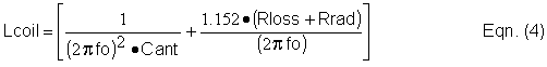
It is important to note that the computed values of C ant and Lcoil do not go resonant at the carrier frequency, fo. If you calculate it out you will get something slightly lower. But more on this oddity in the next section. Lcoil is calculated to be 2.831 mH.
A Critical Modification to the Class-E Transmitter
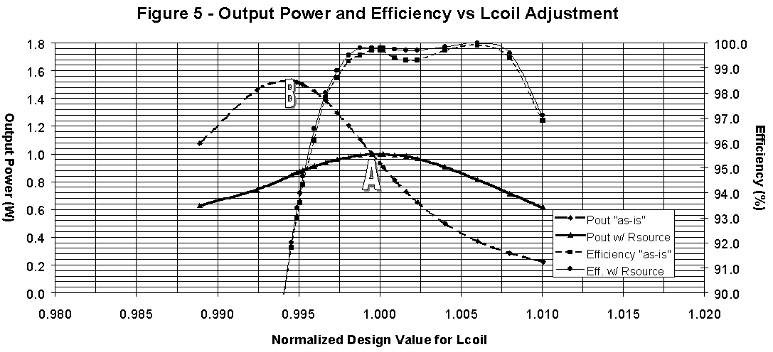
What a surprise! I started running several computer simulations in preparation for building this circuit when I discovered a nasty characteristic of the Class-E design -- at least for how we want to use it. By necessity the LowFER or MedFER installation has a very high-Q. We need to be able to tweak a coil or a cap manually in order to peak the antenna’s RF current to resonance. At first, I assumed that the resonance point of the Class-E design would coincide with its operating point for maximum efficiency. However, this is not true. (See Figure 5 -- each data point represents a specific PSPICE simulation run.) I also tried tweaking the other components to find one that would coincide with maximum efficiency, but no luck. What we need is some easy way to ensure that the antenna current is peaked.
|
Unfortunately, if the design is left ‘as-is’, we will inadvertently mis-tune the transmitter as follows:
Step 1 – we correctly design the circuit according to the design formulas. This puts us at point “A” on the dashed-bold line of Fig. 5.
Step 2 – we tweak Lcoil to maximize the RF antenna current. (I use a RF ammeter in series with Lcoil for this purpose. See article [13] on how to build one.) We do this to ensure maximum radiated power, but look at what happens when Lcoil is varied. The ‘peaked’ value (0.994 x Design value) of Lcoil is slightly less inductive than the design value, so we end up at point “B” on the graph. Ordinarily this would not be a problem except that the efficiency (thin-dashed line) drops to 90% at this operating point. Also note that the output power has increased from the design value of 1.0 watt up to 1.52 watts. (The input power is now at 1.69 watts.) So here comes
Step 3 whether we like it or not – we must lower Vdd to
maintain the input power at ![]() 1.0 watt due to Part 15 regulations. Only now, we no
longer have an output power of ~1.0 watt. We have 900 milliwatts
at best. Also, look at the narrow tuning range for peaking the
output power. A 1% change in the value of Lcoil causes a whopping
4.6 dB drop in output power. This is a very sensitive adjustment!
We really don’t wanna chase the tuning around as the outside
temperature changes. Obviously we can’t just leave the
circuit at point “A” and expect it to
remain there. We have to be able to peak the antenna current
periodically to keep it there.
1.0 watt due to Part 15 regulations. Only now, we no
longer have an output power of ~1.0 watt. We have 900 milliwatts
at best. Also, look at the narrow tuning range for peaking the
output power. A 1% change in the value of Lcoil causes a whopping
4.6 dB drop in output power. This is a very sensitive adjustment!
We really don’t wanna chase the tuning around as the outside
temperature changes. Obviously we can’t just leave the
circuit at point “A” and expect it to
remain there. We have to be able to peak the antenna current
periodically to keep it there.
So, what can we do to fix this problem? I suppose that we could add a circuit that multiplies the input current times the supply voltage and varies the voltage so that exactly one-watt is applied to the transmitter. This sounds rather complicated, especially when you consider loop-stability with on/off keying for CW, but it would solve the problem of inadvertently tuning Lcoil to point “B”.
After pondering the situation for a while, I came up with an easier solution that involves only one additional resistor. The concept is simple. Recall that for maximum power transfer between source and load, you want a complex-conjugate match. At DC this says that the source resistance should equal the load resistance. For those who have not seen the derivation, I will repeat it here, for this is a simple yet important concept to make the Class-E circuit friendly.
We start with the circuit shown in Figure 6. A voltage source, Vs, feeds two resistances, Rsource and Rload. Given that there is some non-zero value of resistance for Rsource, what is the optimum value for Rload such that it dissipates the maximum possible power? If Rload is small, then the power dissipated is still small. If Rload is large, then the current through it is small and the power dissipated is still small. A maximum value lies somewhere in between, but where?
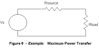 |
Using Fig. 6 the expression for the power in Rload is:

Holding Rsource constant, we take the derivative of this expression with respect to Rload. We then set it equal to zero to find a maximum (as Rload varies):
Taking the partial derivative:

With this in mind, we are going to deliberately waste 1 watt in order to tame the Class-E circuit and get our ~100 % efficiency back again. Here’s how: We feed the circuit with double the supply voltage (2 x Vdd) through a resistor (Rsource) that is equal to the load resistance (Vdd / Irfc) as seen by the original DC supply (Vdd). Refer to Figure 7:
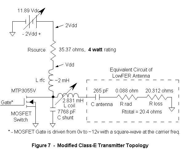 |
The DC load presented by the transmitter at Lrfc is equivalent to the load resistor (Rload) of Fig. 6. (Rload is not to be confused with Rrad or Rloss.) So now we are feeding the transmitter the same voltage as before (Vdd) at the same current as before (Irfc). Therefore the maximum possible input power is one watt. If anything changes from optimum with the transmitter circuit, the input power will drop. The result is shown on the graph. Refer back to the solid-bold line at point “A” of Fig. 5. Now the Class-E transmitter is well behaved as we peak the antenna current. A 1% change in the value of Lcoil results in only a 2 dB drop in output power. Note that design point “A” is now located at peak output power, where the efficiency (thin-solid line) is 99.8%. Rsource can be calculated using Equation (10) and is 35.37 ohms in this case.

We are supplying two watts to the overall circuit. One watt is dissipated by Rsource and the other watt flows into the transmitter, where virtually all of it is converted to RF power for the antenna. (Of course, the antenna only radiates ~ 2 milliwatts into the ether, but that is another subject.) This complies with the spirit and intent of Part 15 in that only one watt is delivered to the final stage. We have sacrificed the extra watt in heating the resistor. Obviously you would never do this with a high-power transmitter where 50% overall efficiency would generate a lot of heat, but for our purposes, it is an excellent solution. But let’s give proper credit where credit is due. While looking up references, I stumbled upon Lyle Koehler’s article [14] on this very same technique. I guess that proves that good designs never die, they just get reinvented.
Intuitively we can see why Rsource works so well. If the transmitter draws too little dc current, then the voltage drop across Rsource is smaller, and a higher voltage is applied to the transmitter. This tends to get it operating at higher power. And alternatively, if the transmitter draws too much current, then more voltage drops across Rsource, reducing the voltage available to the transmitter. This is classic negative feedback. Note that you should parallel and/or series several resistors together when creating Rsource so that it has a 4 watt rating or higher. Should the transmitter short, Rsource will dissipate four watts.
Computer Simulation Results
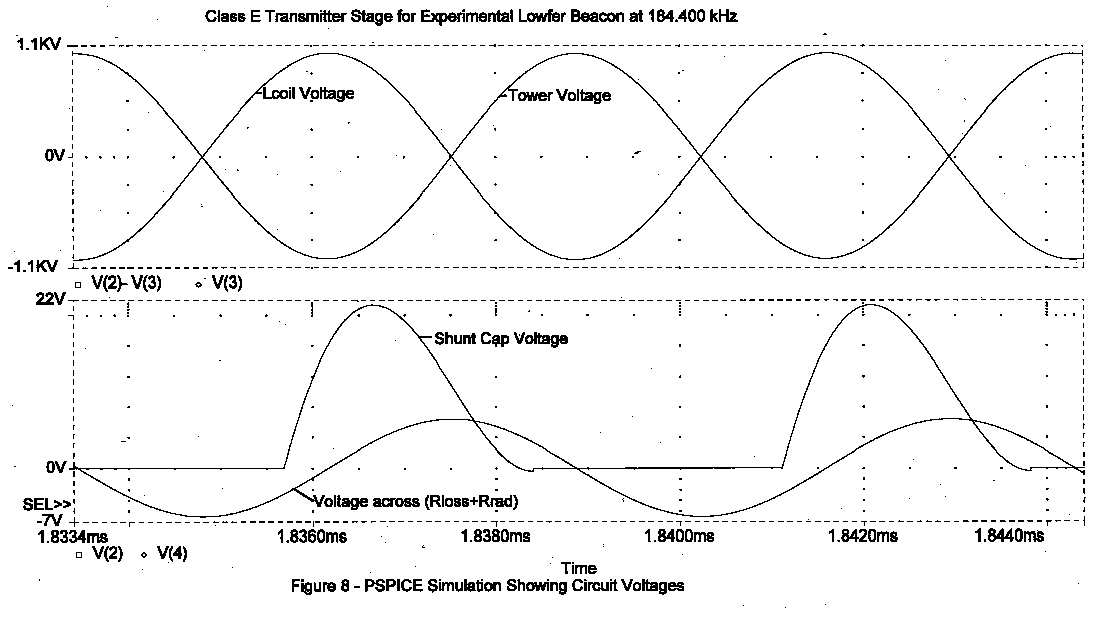
SPICE is an acronym for Simulation Program with Integrated Circuit Emphasis. The evaluation copy of MicroSim’s PSPICE is available at no charge to professionals and engineering students by calling (800) 245-3022. The software is very handy. An excellent reference book on how to use PSPICE is listed in [15]. The modified Class-E transmitter of Fig. 7 has been simulated with Lrfc = 2 mH. The results are shown in this section. See Fig. 4 for circuit currents. Circuit voltages are shown in Figure 8. Note that the voltage across Lcoil is 1,020 Vac peak (that’s 1.02 kV!), so watch the lead dressing and keep the two ends of the Litz wire separated to prevent arcing. Don’t use connectors or binding posts anywhere – wire everything directly using high-voltage insulated wire. This will preserve the antenna’s “Q” in humid weather. For this example, the antenna current is 312 mA peak with a Q of 160. The tower voltage is also 1,020 Vac peak, which is why glass insulators are used to insulate the tower.
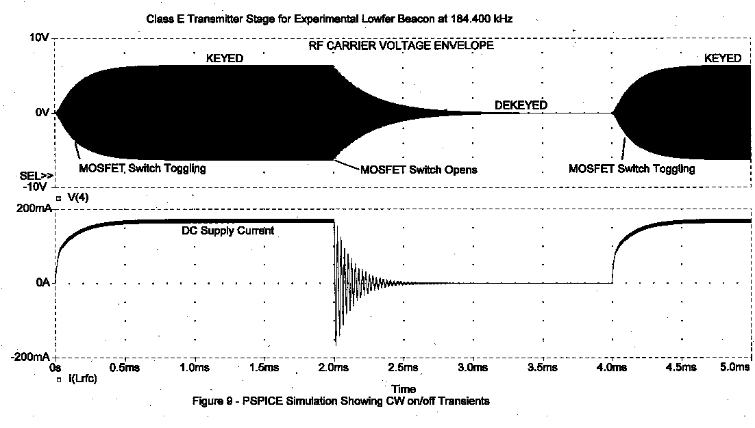
I also decided to simulate the effects of transient turn-on (key) and transient turn-off (dekey). See Figure 9. It takes 357 microseconds for the transmitter to come up to 90% of full power, and 631 usec to decay to 10% of full power when dekeyed. Note the ringing in the DC supply line during dekey. This occurs because Lrfc and Cshunt form part of a low-frequency resonant circuit (39 kHz) when the switch remains open.
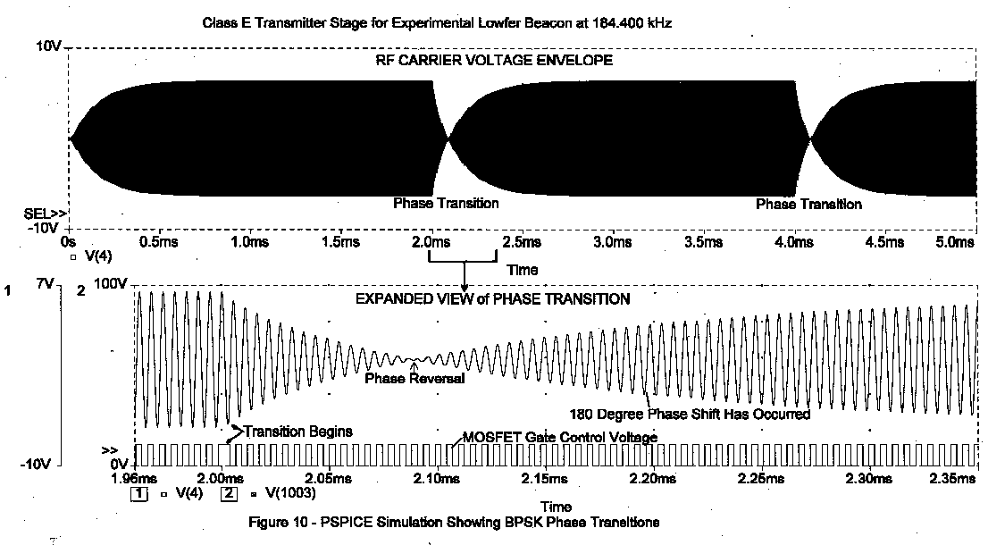
I also decided to model the effects of differential BPSK modulation. The switching square-wave pulse-train to the MOSFET gate is suddenly inverted, which causes the output power to quickly decay and then build back up again, only now with a 180- degree phase shift. This is shown in Figure 10. It takes only 90 usec for the waveform to decay to zero and another 347 usec for it to build back up to 90%, for a total BPSK transient of 437 usec.
 |
 |
 |
The value of Lrfc is not critical, preferably between 0.5 and 5 mH, but it should have a reactance of at least ten times (Rloss + Rrad). Since Lrfc does not carry any appreciable ac current, there should be no core loss to worry about. Larger values of Lrfc result in longer but negligible attack and decay times for CW keying (Fig. 9). Smaller values result in larger ac ripple riding on top of the DC supply current (Irfc) when keyed. (If you look closely at Fig 9, you will see about 10 mAac peak-to-peak ripple riding on the DC Supply Current.) You can even include the dc resistance, inherent in winding Lrfc, as part of Rsource. Just make sure to document everything properly. You will have to measure the voltage drop across Rsource and compute some numbers to verify that you have complied with the Part 15 one-watt limit.
Part values have been shown to four significant digits, but only to assist the reader in repeating the calculations. Such accuracy is not needed. Actual values are not too critical as the design is robust to variation. In Figs. 4 & 8, you may have noticed that the shunt cap voltage waveform is not quite optimum, yet efficiency is still 99.8%.
References
[1] – The Northern Observer, #14, 1989, “A Class-E Beacon Transmitter for the LowFER Band”, pp. 5-8, by Greg Raven (TEXAS) & KF5N.
[2] – PSPICE electronic circuit simulator, MicroSim Evaluation copy, Release 8.
[3] – The LOWDOWN, Feb 96, “Low Frequency Coil Q”, pp. 27-29, by Bill Bowers.
[4] – The LOWDOWN, Jul 96, “Coils, Coils, Coils”, pp. 21-22, by Bill Bowers.
[5] – The LOWDOWN, Aug 97, “The TEXAS Beacon Part 1 of 3”, pp. 20-27 by Bill Cantrell.
[6] – IEEE Journal of Solid State Circuits, Feb. 69, “Frequency and Power Limitations of Class D Transistor Amplifiers,” SC-4, pp. 25-37, by Chudobiak and Page.
[7] – Solid State Radio Engineering, 1980, pp. 448-454, by Krauss, Bostian, & Raab.
[8] – IEEE Journal of Solid State Circuits, June 75, “Class E, a New Class of High- Efficiency Tuned Single-Ended Power Amplifiers,” SC-10, pp. 168-176, by N. O. Sokal and A. D. Sokal.
[9] – IEEE Transactions on Circuits and Systems, Dec. 77, “Idealized Operation of the Class E Tuned Power Amplifier”, CAS-24, pp. 725-735, by F. H. Raab.
[10] – IEEE Journal of Solid State Circuits, Apr. 78, “Effects of Circuit Variations on the Class E Tuned Power Amplifier”, SC-13, pp. 239-247, by F. H. Raab.
[11] – “Coupling the VLF Antenna to the Transmitter”, by Ed Phillips W6IZJ, and related articles in “Transmitting Antennas & Ground Systems for 1750 Meters”, edited by Michael Mideke, Nov 1987.
[12] – “Basic 1750M Transmitting Antenna”, by Mitchell Lee, and related articles in “Transmitting Antennas & Ground Systems for 1750 Meters”, edited by Michael Mideke, Nov 1987.
[13] – “RF Ammeter for 1750M Transmitting Antennas”, by Mitchell Lee, et. al., in [12].
[14] – The LOWDOWN, Feb 96, “Simple Transmitter Power Limiter”, p. 25-26, by Lyle Koehler.
[15] – SPICE for Circuits And Electronics Using PSPICE, 1990, by M. H. Rashid.
Contents of this website are (c)1997-99 of K3PGP and of the originating authors.
NOTE: You may link to this page but you may NOT copy without permission from the author and K3PGP.
To contact the author of this article: Email Bill Cantrell
-=<EOF>=-