This collection includes power supplies suitable for almost any HeNe tube or laser head with an optical output power from .5 to 35 mW - and beyond. And, these circuits can be easily modified for your specific needs: For example, a very high power HeNe tube or a weird laser requiring multiple power supply feeds and separate starters.
WARNING: There are so many complete HeNe power supply schematics in this one document that their combined mass may cause a singularity to form inside your computer. :-) The lawyers made me include this statement - honest. ;-)
Note: For an explanation of the meanings of various designations like X, Y, HV+, Tube-, etc., used in these schematics, see the section: Notation used in HeNe Power Supply Diagrams and Schematics.
Many of these designs are quite old since modern commercial units tend toward inverter designs since they can be more compact and have higher efficiency. Unfortunately, modern inverter types are nearly always potted in Epoxy and impossible to disassemble and analyze. However, AC Line operated power supplies will drive HeNe tubes just as well as fancy inverters and are somewhat easier to construct and troubleshoot (especially for high power designs).
The line side circuitry is not shown for any of these. See the section: AC Input Circuitry for HeNe Power Supplies for details.
Those with "Sam's" in the title were built using mostly scrounged parts like tube type TV power transformers that had been minding their own business in various storage cabinets often for many many years. My total cost for the remaining components for each power supply was generally not over $5.
Estimated specifications (Edmund Scientific):
This is the power supply I traced out and measured which is in an Edmund Scientific 0.5 mw. Laser circa probably around 1975. I bought a 1 mW. tube (1986) when the old one broke. It is still running just fine. I think it is a rather clever design and I don't think they come any simpler.
       X                   C5                      C7
       +-------------------||-----------+----------||-----------+---o HV+
       |                       D7  D8   |  D9  D10     D11 D12  |   R5
       |                    +--|>|-|>|--+--|>|-|>|--+--|>|-|>|--+--/\/\--+
       |  D1  D2  D3   Y    |          C6           |              18K   |
   +---+--|>|-|>|-|>|--+----+----------||-----------+               1W   / R6
||(    |               |    |                                            \ 33K
||(    |          C1 +_|_   / R1                                         / 1W
||(    |       4.7uF  ---   \ 1M                                         |
||(    |        450V - |    /                                            / R7
||(    |               |    |                                            \ 33K
||(    |               +----+ W   Transformer: 650 VRMS, 20 mA           / 1W
||(    |               |    |       (primary not shown)                  |
||(    |          C2 +_|_   / R2                                         / R8
||(    |       4.7uF  ---   \ 1M                                         \ 33K
||(    |        450V - |    /                                            / 1W
||( T  |               |    |     D1-D7: 1N4007 or similar               |
   +-------------------+----+                                            / R9
       |               |    |                                            \ 33K
       |          C3 +_|_   / R3  C1-C4: 4.7uF, 450V                     / 1W
       |       4.7uF  ---   \ 1M  C5-C7: .001uF, 2KV                     |Tube+
       |        450V - |    /                                          .-|-.
       |               |    |     R1-R4: 1M, 1W                        | | |
       |               +----+ Z   R5-R9: (ballast, 18K+4x33K, 1W)      |   |
       |               |    |                                      LT1 |   |
       |          C4 +_|_   \ R4                                       |   |
       |       4.7uF  ---   / 1M                                       ||_||
       |        450V - |    \                                          '-|-'
       |               |    |                                            |Tube-
       +--|<|-|<|-|<|--+----+--------------------------------------------+---o
          D4  D5  D6                                                    _|_ HV-
                                                                         -
Note that there are no equalizing resistors across the 1N4007s. While I have
been building similar supplies without them, the use of 10M resistors across
each diode to equalize the voltage drops is recommended.
The 650 V transformer output feeds a voltage doubler (D1 to D6 and C1 to C4) resulting in about 1,750 V across all the electrolytics. (Slightly less than 2 times the peak value of 650 VRMS.)
D7 to D12 and C5 to C7 form a classical voltage multiplier ladder which generates a peak of up to 4 * V(peak) + 2 * V(peak) or 6 * 880 = 5,300 V. This seems somewhat low but the power supply is for only a .5 mW tube. See the section: Voltage Multiplier Starting Circuits for a description of its design and operation.
The 150K ballast resistor is actually constructed from 4 - 33K resistors and one 18K resistor in series. It doesn't have to be, but this is convenient and allows the ballast to be changed easily (or just tap off the appropriate point for your tube. My notes show 600 V across the ballast resistor-combo.
The ballast resistor should be located close to the tube with as short a lead as possible and as little capacitance to surroundings as possible. The tube needs to see a high impedance source. This isn't super critical, but keep the wire down to 1 to 3 inches and the first few resistors away from any case or ground material.
Since there is no active regulator, the tube current will depend on the power line voltage and other factors like temperature. However, the relatively large ballast resistor in this power supply should minimize excessive variation.
Estimated specifications (SP-155):
       X             C103
       +--------------||-------------+
       |             C100            |       C101
       +--------------||-------------+--------||---------+---o HV+
       |                      CR101  |   CR102    CR103  | R107 (Rbp)
       |                   +---|>|---+---|>|---+---|>|---+---/\/\---+
T100   |    CR100    Y     |        C102       |             33K    |
   +---+-----|>|-----+-----+---------||--------+              2W    /
||(                  |     |                                        \ Rba
||(           C103 +_|_    / R100                                   /
||(           10uF  ---    \ 470K   T100: 1,300 VRMS, 20mA          \
||(           450V - |     / 1W       (primary not shown)           |
||(                  |     |                                        |Tube+
||(                  +-----+ W      CR100-CR103: LMS60 (6KV)      .-|-.
||(                  |     |                                      |   |
||(           C104 +_|_    / R101   C100-C103: 560pF, 6KV         |   |
||(           10uF  ---    \ 470K   C103-C105: 10uF, 450V         |   | LT100
||(           450V - |     / 1W                                   |   |
||( T                |     |        R100-R103: 470K, 1W           |   |
   +---+             +-----+        R107 (ballast): 33K, 2W       ||_||
       |             |     |                                      '-|-'
       |      C105 +_|_    / R102                                   |Tube-
       |      10uF  ---    \ 470K                +------------------+
       |      450V - |     / 1W                  |                 _|_
       |             |     |    R103           |/ C Q100            -
       |             +-----+----/\/\------+----|    MJE3439
       |             |     Z    430K      |    |\ E
       |      C106 +_|_          1W       |      |
       |      10uF  ---                  _|_,    /
       |      450V - |            CR104 '/_\     \ R106
       |             |          1N5241B   |      / 2.74K
       |             |                    |      \
       |             |                    |      |
       +-------------+--------------------+------+---o HV-
The 1,300 V transformer output feeds a half wave rectifier (CR100) and filter
resulting in about 1,750 V across all the electrolytics. (Slightly less than
the peak value of 1,300 VRMS.)
CR101 to CR103 and C100 to C103 form a classical voltage multiplier ladder which generates a peak of up to 4 * V(peak) + 2 * V(peak) or 6 * 1,750 = 10,600 but losses in the diode-capacitor network probably reduce this somewhat. See the section: Voltage Multiplier Starting Circuits for a description of its design and operation.
Q100, CR104, and R106 form a constant current regulator which will attempt to maintain the tube current at (Vz - .7)/R106 or about 3.75 mA in this case. Its compliance range is about 300 V. This can easily be adapted to your requirements by either changing CR104 or R106 appropriately.
The anode ballast resistor, Rba, needs to be large enough to maintain stability (at least 75K-33K=42K or so in this case) and should be as close to the HeNe tube as possible. Commercial laser heads generally include an internal 75K ballast resister. See the section: Ballast Resistors, Function, Selecting for more information.
Estimated specifications (SP-247):
       X    R1       C1                   C11
       +---/\/\------||----------+---------||--------+
       |   680K           CR3    |   CR4       CR5   |  CR6
       |              +---|>|----+---|>|---+---|>|---+---|>|---+
T1     |   CR1   Y    |        C10         |    C12            |
   +---+---|>|---+----+---------||---------+-----||-----+------+----+---o HV+
||(    |         |    |                                 |      |    |
||(    |    C2 +_|_   / R2                              |  R11 /    |
||(    |  10uF  ---   \ 680K  T1: 1,200 VRMS, 20mA      | 120K \    |
||(    |  500V - |    / 1W      (primary not shown)     |   2W /    |
||(    |         |    |                                 |      |  |/ C Q1
||(    |         +----+ W     CR1-CR6: SCM60, 6KV       |      +--|    MJE3439
||(    |         |    |                                 |      |  |\ E
||(    |    C3 +_|_   / R3    C2-C9: 10uF, 500V         |  R12 /    |
||(    |  10uF  ---   \ 680K  C1, C10-C13: 500pF, 6KV   | 120K \    |
||(    |  500V - |    / 1W                              |   2W /    |
||(    |         |    |       R2-R9: 680K, 1W           |      |  |/ C Q2
||(    |         +----+       R11-R14: 120K, 2W         |      +--|    MJE3439
||(    |         |    |                                 |      |  |\ E
||(    |    C4 +_|_   / R4    Q1-Q4: MJE3439            |  R13 /    |
||(    |  10uF  ---   \ 680K                            | 120K \    |
||(    |  500V - |    / 1W                              |   2W /    |
||(    |         |    |                                 |      |  |/ C Q3
||(    |         +----+              +------------------+      +--|    MJE3439
||(    |         |    |              |                         |  |\ E
||(    |    C5 +_|_   / R5           |                     R14 /    |
||(    |  10uF  ---   \ 680K         |                    120K \    |
||(    |  500V - |    / 1 W          |                      2W /    |
||( T  |         |    |              |             R10 48K     |  |/ C Q4
   +---|---------+----+              |            +----/\/\----+--|    MJE3439
       |         |    |              |            |            |  |\ E
       |    C6 +_|_   / R6           |            |          |/ E   |
       |  10uF  ---   \ 680K         |            +----------|      |
       |  500V - |    / 1W           |            |       Q5 |\ C   |
       |         |    |              |      ZD1  _|_, 2N5086   |    |
       |         +----+         C16 _|_ 1N5245A '/_\           +----+
       |         |    |      .047uF ---           |   R17           |
       |    C7 +_|_   / R7      6KV  |            |  5K 1W   R16    |
       |  10uF  ---   \ 680K         |     Adjust +---/\/\---/\/\---+
       |  500V - |    / 1W           |            |    |     1.5K
       |         |    |              |   +--------+----+
       |         +----+              |   |   R15    R18       Rba
       |         |    |              |   +---/\/\---/\/\---+--/\/\--+
       |    C8 +_|_   / R8           |       20K    20K             |Tube+
       |  10uF  ---   \ 680K         |        2W     2W           .-|-.
       |  500V - |    / 1W           |   <------ Rbp ------>      | | |
       |         |    |              |                            |   |
       |         +----+ Z       C15 _|_                           |   | LT1
       |         |    |      .047uF ---                           |   |
       |    C9 +_|_   / R9      6KV  |                            |   |
       |  10uF  ---   \ 680K         |                            ||_||
       |  500V - |    / 1W           |                            '-|-'
       |         |    |              |                              |Tube-
       +---|<|---+----+--------------+------------------------------+---o HV-
           CR2                                                     _|_
                                                                    -
The 1,200 V transformer output feeds a voltage doubler consisting of rectifiers
CR1 and CR2 and filter capacitors C2 through C9 resulting in about 3,200 V
across all the electrolytics. (Slightly less than 2 times the peak value of
1,200 VRMS.)
CR3 to CR6 and C1 and C10 through C12 form a classical voltage multiplier ladder which generates a peak output of 4 * V(peak) + 2 * V(peak) or 6 * 1,700 = 10,200 V but losses in the diode-capacitor network probably reduce this slightly. See the section: Voltage Multiplier Starting Circuits for a description of its design and operation.
C15 and C16 provide some additional filtering to the output so unlike the previous supplies whose outputs include the last multiplier diodes without filtering, this one is more pure DC. This would be better for laser communications, for example, as the tube current will have less ripple. However, it may not matter for a basic power supply so you could probably get away without having to find/construct this high voltage capacitor.
Q1 through Q5, their associated resistors, and ZD1 (15 V zener) maintains a constant voltage of 15 V across the combination of R16 + R17 so the tube current will be 15/(R16 + R17). For example, with the R17 set for 1.5 K, the tube current will be 5 mA. The adjustment range is approximately 2.3 to 10 mA. The voltage compliance range of this power supply should be over 1,000 V.
Keep in mind that if you include this high side regulator, it must be insulated to handle the full starting voltage. An alternative that might be easier to construct would be use this operating/starting voltage design but to substitute a similar compliance low-side regulator.
The anode ballast resistor, Rba, needs to be large enough to maintain stability (at least 75K-40K=35K or so in this case) and should be as close to the HeNe tube as possible. Commercial laser heads generally include an internal 75K ballast resister. See the section: Ballast Resistors, Function, Selecting for more information.
(Model number PS1 is arbitrary - supply was unmarked).
Estimated specifications (AT-PS1):
       X    R9     C9            C11             C13             C15
       +---/\/\----||-----+-------||------+-------||------+-------||------+
       | 100K, 1 W  CR3  |  CR4     CR5  |  CR6     CR7  |  CR8     CR9  | HV+
       |         +--|>|--+--|>|--+--|>|--+--|>|--+--|>|--+--|>|--+--|>|--+--o
T1     |   CR1   |Y              |               |               |       |
   +---+---|>|---+----+----||----+-------||------+-------||------+       |
||(    |         |    |   C10           C12             C14              |
||(    |    C1 +_|_   / R1                                           R10 /
||(    |  10uF  ---   \ 510K  T1: 750 VRMS, 20 mA                  (Rbp) \
||(    |  450V - |    / 1W      (primary not shown)                  47K /
||(    |         |    |                                               5W \
||(    |         +----+       CR1-CR9: 3KV                               |
||(    |         |    |                                                  |
||(    |    C2 +_|_   / R2    C1-C8: 10uF, 450V                       +--+
||(    |  10uF  ---   \ 510K  C9-C15: .005uF, 3KV                     |
||(    |  450V - |    / 1W                                            |
||(    |         |    |       R1-R8: 510K                             /
||(    |         +----+                                            Rb \
||(    |         |    |                                               /
||(    |    C3 +_|_   / R3                                            \
||(    |  10uF  ---   \ 510K                                          |
||(    |  450V - |    / 1W                                            |Tube+
||(    |         |    |                                             .-|-.
||(    |         +----+                                             | | |
||(    |         |    |                                             |   |
||(    |    C4 +_|_   / R4                                          |   |
||(    |  10uF  ---   \ 510K                                        |   | LT1
||(    |  450V - |    / 1W                                          |   |
||( T  |         |    |                                             |   |
   +---|---------+----+                                             |   |
       |         |    |                                             ||_||
       |    C5 +_|_   / R5                                          '-|-'
       |  10uF  ---   \ 510K                                          |Tube-
       |  450V - |    / 1W                                            |
       |         |    |                                               +----+
       |         +----+                                               |   _|_
       |         |    |                                               |    -
       |    C6 +_|_   / R6                                            |
       |  10uF  ---   \ 510K                                          |
       |  450V - |    / 1W                                            |
       |         |    |                                               |
       |         +----+                                               |
       |         |    |                                          +----+
       |    C7 +_|_   / R7                            MJE2360T   | C  |
       |  10uF  ---   \ 510K                                   |/     |
       |  450V - |    / 1W                         +-----------| Q1   |
       |         |    |              R8            |           |\     |
       |         +----+-------------/\/\-----------+             | E  |
       |         |    Z             470K           |         R11 /    / R12
       |    C8 +_|_                  1W      ZD1  _|_,      3.6K \    \ 375K
       |  10uF  ---                       1N4744 '/_\            /    / 2W
       |  450V - |                           15V   |             |    |
       |         |                                 |             |    |
       +---|<|---+---------------------------------+-------------+----+---o HV-
           CR2
Note: the laser head itself may have an additional ballast resistor (not
shown).
The 750 V transformer output feeds a voltage doubler consisting of rectifiers CR1 and CR2 and filter capacitors C1 through C8 resulting in about 2,000 V across all the electrolytics. (Slightly less than 2 times the peak value of 750 VRMS.)
CR3 to CR9 and C9 through C15 form a classical voltage multiplier ladder which generates a peak of 2 * V(peak) + 8 * V(peak) or 10 * 1,000 = 10,000 V but losses in the diode-capacitor network probably reduce this somewhat. See the section: Voltage Multiplier Starting Circuits for a description of its design and operation.
Q1, ZD1, R8, and R11 form the low-side current regulator. The tube current will be (15-.7)/R11 or just about 4 mA. So, for a different current, select R11 to be 14.3/I.
Since the voltage compliance range of this power supply is only around 500 V, the ballast resistor will still need to be selected carefully to achieve stable regulation for your particular tube. See the sections beginning with: Selecting the Ballast Resistor for further info.
The anode ballast resistor, Rba, needs to be large enough to maintain stability (at least 75K-47K=38K or so in this case) and should be as close to the HeNe tube as possible. Commercial laser heads generally include an internal 75K ballast resister. See the section: Ballast Resistors, Function, Selecting for more information.
The modified circuit provides a current adjustment control, modulation input, 'Beam On' indicator, and tube current sense test points. I have implemented these changes to the Aerotech PS1 and installed the current adjust pot, jacks for Ground/Test+, Test-, Signal in, and Signal ground, and the Beam On LED on the power supply case.
       |       (Remainder of circuit                                  |Tube-
       |        identical to Aerotech PS1)   +----+-----------+-------+---o +
       |                                     |   _|_          |       |
       |         |    |                      |    -      ZD2 _|_  R13 / Test
       |         +----+                      |        1N4742 /_\   1K \ 1 V/mA
       |         |    |                      |           12V  |       /
       |    C6 +_|_   / R6                   |                |       |
       |  10uF  ---   \ 510K                 |                +-------+---o -
       |  450V - |    / 1W                   |                      __|__ IL2
       |         |    |                      |                      _\_/_ Beam
       |         +----+                      |                        |   On
       |         |    |                      |                    +---+
       |    C7 +_|_   / R7                   |         MJE2360T   | C |
       |  10uF  ---   \ 510K                 |                  |/    |
       |  450V - |    / 1W                   |       +---/\/\---| Q1  |
       |         |    |                      |    T2 |   R15    |\    |
       |         +----+ Z                    +--+    +   15K      | E |
       |         |    |                          )||(             |   |
       |         |    / R8                       )||(             |   / R12
       |         |    \ 470K                     )||(             |   \ 375 K
       |    C8 +_|_   / 1 W      Signal in o----+    +            /   / 2W
       |  10uF  ---   |                          1:1 |        R11 \   |
       |  450V - |    +------------------------------+       1.5K /   |
       |         |                                   |            |   |
       |         |                             ZD1  _|_,    R14   /   |
       |         |                          1N4744 '/_\     5K +->\   |
       |         |                             15V   |  Adjust |  /   |
       |         |                                   |         |  |   |
       +---|<|---+-----------------------------------+---------+--+---+---o HV-
           CR2
Each of the new and improved features is described below:
The phone line coupling transformer from a long forgotten 2400 baud modem served nicely for this application resulting in a useful frequency response from about 100 and 10,000 Hz.
Stay tuned for exciting future developments!
A similar approach can be used with any of the other HeNe power supply designs described in this document which use low-side regulation or which do not have any regulation.
CAUTION: Don't try this with power supplies using high-side regulation either by modifying the regulator (you would need a 15 KV coupling capacitor or 15 KV opto-isolator to hold off the starting pulse) or adding an additional low-side modulator (the two circuits will be fighting each other).
There may have been several versions of this model as I have two slightly different samples using the same circuit board. The one described below which designate model PS2B uses the higher voltage tap on the transformer. A nearly identical design - model PS3A - runs with a transformer secondary of 1,150 VRMS yielding 3,000 VDC operating, 12,000 VDC starting, and uses only 8 electrolytic filter capacitors.
See the section: Aerotech Model PS2A-X HeNe Power Supply (AT-PS2A-X) for its circuit diagram with my modifications.
Estimated specifications (AT-PS2B):
       X   R11    C11           C13             C15             C17
       +---/\/\----||----+-------||------+-------||------+-------||------+
       | 10M, 5 W   CR3  |  CR4     CR5  |  CR6     CR7  |  CR8     CR9  | HV+
       |         +--|>|--+--|>|--+--|>|--+--|>|--+--|>|--+--|>|--+--|>|--+--o
       |         |               |               |               |       |
       |         |    +----||----+-------||------+-------||------+       |
T1     |   CR1   |Y   |   C12           C14             C16              |
   +---+---|>|---+----+                                     +----+-------+
||(    |         |    |                                     |    |
||(    |    C1 +_|_   / R1                              R12 /    |
||(    |  10uF  ---   \ 510K  T1: 1,380 VRMS, 20mA      62K \    |
||(    |  500V - |    / 1W      (primary not shown)      2W /    |
||(    |         |    |                                     |  |/ C Q1
||(    |         +----+       CR1-CR9: 5KV                  +--|    MJE2360T
||(    |         |    |                                     |  |\ E
||(    |    C2 +_|_   / R2    C1-C10: 10uF, 500V        R13 /    |
||(    |  10uF  ---   \ 510K  C11-C17: .005uF, 5KV      62K \    |
||(    |  500V - |    / 1W                               2W /    |
||(    |         |    |       R1-R10: 510K                  |  |/ C Q2
||(    |         +----+       R11-R14: 62K, 2W              +--|    MJE2360T
||(    |         |    |                                     |  |\ E
||(    |    C3 +_|_   / R3    Q1-Q3: MJE2360T           R14 /    |
||(    |  10uF  ---   \ 510K                            62K \    |
||(    |  500V - |    / 1W    U1: LM723                  2W /    |
||(    |         |    |                              R24    |  |/ C Q3
||(    |         +----+                          +---/\/\---+--|    MJE2360T
||(    |         |    |                          |   3.3K   |  |\ E
||(    |    C4 +_|_   / R4                       |        |/ E   |
||(    |  10uF  ---   \ 510K                     +--------|   Q4 | 2N4126
||(    |  500V - |    / 1W                       |        |\ C   | (PNP)
||(    |         |    |                          |    C18   |    |
||(    |         +----+         +--------------+-+----||----+----+
||(    |         |    |         |              |  .005 uF
||(    |    C5 +_|_   / R5     _|_, ZD1        |
||(    |  10uF  ---   \ 510K  '/_\  1N4744     +------------------------+
||(    |  500V - |    / 1W      |   15 V, 1W                            |
||( T  |         |    |         |                                       |
   +---|---------+----+         |          R15 15K   1N4148   |\        | C
       |         |    |         |         +--/\/\--+----------|+ \*   |/*
       |    C6 +_|_   / R6      | +-----+ |R14 15K |  D1      |Err >--|
       |  10uF  ---   \ 510K    | |Vref*|-+--/\/\--|---+---+--|- /    |\  E
       |  500V - |    / 1W      | +-----+ 7.15V    |   |   |  |/        |
       |         |    |         |                  |   |   |        R21 /
       |         +----+         |              +---+   |   \ R16    10K \
       |         |    |         |              |   |  _|_  / 82K        /
       |    C7 +_|_   / R7      |         C19 _|_  /  /_\  \      ZD2   |
       |  10uF  ---   \ 510K    |        .1uF ---  \   |   |   1M4733  _|_,
       |  500V - |    / 1W      |              |   /   |   |     5.1V '/_\
       |         |    |         |              |   |   |   |            |
       |         +----+         +--------------+---+---+----------------+
       |         |    |         |               R17 15K    | R25 (Rbp)
       |    C8 +_|_   / R8      |   R20      R19           |  47K 5W
       |  10uF  ---   \ 510K    +-+-/\/\-----/\/\----------+---/\/\---+
       |  500V - |    / 1W        |   | 1.5K  1.8K                    |
       |         |    |           +---+                               /
       |         +----+        Current Adjust                      Rb \
       |         |    |         (6 to 11 mA)                          /
       |    C9 +_|_   / R9                                            |Tube+
       |  10uF  ---   \ 510K       Note: Components marked          .-|-.
       |  500V - |    / 1W          with '*' are part of            | | |
       |         |    |             U1, LM723.  (Compensation       |   |
       |         +----+ Z           not shown.)                     |   | LT1
       |         |    |                                             |   |
       |   C10 +_|_   / R10                                         |   |
       |  10uF  ---   \ 510K                                        ||_||
       |  500V - |    / 1 W                                         '-|-'
       |         |    |                R23                            |Tube-
       +---|<|---+----+-------------+--/\/\--+------------------------+---o HV-
           CR2                      |   1K   |                       _|_
                                  - o  Test  o +                      -
                                      1 V/mA
The 1,380 V transformer output feeds a voltage doubler consisting of rectifiers
CR1 and CR2 and filter capacitors C1 through C10 resulting in about 3,600 V
across all the electrolytics. (Slightly less than 2 times the peak value of
1,380 VRMS.)
CR3 to CR9 and C11 through C17 form a classical voltage multiplier ladder which generates a peak starting voltage of up to 2 * V(peak) + 8 * V(peak) or 10 * 1,800 = 18,000 V but losses in the diode-capacitor network probably reduce this somewhat. See the section: Voltage Multiplier Starting Circuits for a description of its design and operation.
Q1 through Q4, their associated resistors, and U1 (LM723) maintain a constant voltage of 22 V across the combination of R19 + R20 so the tube current will be 22/(R16 + R17). For example, with the R17 set for 750 ohms, the tube current will be 6.3 mA. The adjustment range is approximately 5 to 9 mA. The voltage compliance range of this power supply is about 800 V at 5 mA (possibly a couple hundred volts greater at higher currents).
The anode ballast resistor, Rba, needs to be large enough to maintain stability (at least 75K-47K=38K or so in this case) and should be as close to the HeNe tube as possible. Commercial laser heads generally include an internal 75K ballast resister. See the section: Ballast Resistors, Function, Selecting for more information.
Estimated specifications (AT-PS2A-X):
      X   R11    C11           C13             C15             C17
      +---/\/\----||----+-------||------+-------||------+-------||------+
      | 10M, 5 W   CR3  |  CR4     CR5  |  CR6     CR7  |  CR8     CR9  | HV+
      |         +--|>|--+--|>|--+--|>|--+--|>|--+--|>|--+--|>|--+--|>|--+--o
      |         |               |               |               |       |
      |         |    +----||----+-------||------+-------||------+       /
T1    |   CR1   |Y   |   C12           C14             C16              \ Rb
   +--+---|>|---+----+                                                  /
||(   |         |    |       T1: 1,150 VRMS, 20mA                       |Tube+
||(   |    C1 +_|_   / R1      (primary not shown)                    .-|-.
||(   |  10uF  ---   \ 510K                                           |   |
||(   |  500V - |    / 1W    CR1-CR9: 5KV                             |   |
||(   |         |    |                                                |   |
||(   |         +----+       C1-C4, C6-C9: 10uF, 500V             LT1 |   |
||(   |         |    |       C11-C17: .005uF, 5KV                     |   |
||(   |    C2 +_|_   / R2                                             ||_||
||(   |  10uF  ---   \ 510K  R1-R4, R6-R9: 510K                       '-|-'
||(   |  500V - |    / 1W    RX1-RX3: 100K, 2W                          |Tube-
||(   |         |    |                                                  |
||(   |         +----+       QX1-QX3: MPSU60        +---------+-------+-+--o +
||(   |         |    |                             _|_        |       |
||(   |    C3 +_|_   / R3                           -   ZD2  _|_, R12 / Test
||(   |  10uF  ---   \ 510K                          1N4742 '/_\   1K \ 1 V/mA
||(   |  500V - |    / 1W                               12V   |       /
||(   |         |    |                           Beam On      |       |
||(   |         +----+             +-----------+---|<|--------+-------+----o -
||(   |         |    |             |           | IL2 LED  R13    R14
||(   |    C4 +_|_   / R4          |           |    +---/\/\---/\/\---+
||(   |  10uF  ---   \ 510K        |           |    |    | 5K   1.5K  |
||(   |  500V - |    / 1W          |           +----+----+ Range      |
||(   |         |    |             |           |    |                 |
   +--|---------+----+             |           |    |        Q1  +----+
      |         |    |             |           |    |    2N3904  |    |
      |    C6 +_|_   / R6          |     ZD1  _|_,  \    (NPN) |/ C   |
      |  10uF  ---   \ 510K        |  1N4744 '/_\   /<---------|      |
      |  500V - |    / 1W          |     15V   |    \ R15      |\ E   |
      |         |    |             |           |    | 500K       |  |/ E QX1
      |         +----+             |           |    | Adjust     +--|  MPSU60
      |         |    |             |           |    |            |  |\ C (PNP)
      |    C7 +_|_   / R7          |           +----+----/\/\----+    |
      |  10uF  ---   \ 510K        |                |  R16 10K        |
      |  500V - |    / 1W          / R17            |                 |
      |         |    |             \ 100K           |    RX1        |/ E QX2
      |         +----+             /                +----/\/\----+--|  MPSU60
      |         |    |             |                   100K      |  |\ C (PNP)
      |    C8 +_|_   / R8          |                    2W   RX2 /    |
      |  10uF  ---   \ 510K        |                        100K \    |
      |  500V - |    / 1W          |                          2W /    |
      |         |    |             |                             |  |/ E QX3
      |         +----+            _|_ C18                        +--|  MPSU60
      |         |    |            --- 100pF                      |  |\ C
      |    C9 +_|_   / R9          |                         RX3 \    |
      |  10uF  ---   \ 510K        |                        100K /    |
      |  500V - |    / 1W          |                          2W \    |
      |         |    |             |                             |    |
      +---|<|---+----+-------------+-----------------------------+----+--o HV-
          CR2
Note: The total ballast resistance, Rb, should be 75K or more to maintain
stability. It is desirable for there to be at laest 20K in the power supply
itself (Rbp) to provide short circuit protection. The remainder (Rba) should
be as close to the HeNe tube anode as possible. Commercial laser heads
generally include an internal 75K ballast resister. See the section:
Ballast Resistors, Function, Selecting for
more information.
The 1,150 V transformer output feeds a voltage doubler consisting of rectifiers CR1 and CR2 and filter capacitors C1 to C4 and C6 to C9 resulting in about 3,000 V across all the electrolytics. (Slightly less than 2 times the peak value of 1,150 VRMS.)
CR3 to CR9 and C11 through C17 form a classical voltage multiplier ladder which generates a peak starting voltage of up to 2 * V(peak) + 8 * V(peak) or 10 * 1,500 = 15,000 V but losses in the diode-capacitor network probably reduce this somewhat. See the section: Voltage Multiplier Starting Circuits for a description of its design and operation.
Current adjust (R15) and current range (R13) pots have been added, the latter being set by a screwdriver. This allows fairly linear control of tube current up to the set limit from the front panel. The minimum current is determined by what bypasses the transistors and passes through the base resistors. This will be up to 3 mA depending on operating conditions.
As desribed in the section: Enhancements to AT-PS1, a current test point and 'Beam-On' indicator have also been added.
The NPN transistor (Q1) buffers the reference voltage so that the very low current source from R15 can drive the base of the pass transistor cascade.
The base resistors, RX1 through RX3 equally distribute the voltage across the 3 PNP pass transistor, QX1 to QX3. The respective transistors act as emitter followers and maintain approximately the same voltages across their C-E terminals. Within the compliance range, the voltage across R13+R14 will be nearly equal to the voltage on the wiper of R15.
R17 and C18 act as a snubber to protect the transistor cascade from the initial over voltage when the tube fires but before the regulator can turn on. I do not know whether this is needed or how much if any it would protect the pass transistors when operating near their maximum ratings.
Three pass transistors are shown here only because that particular number fit conveniently into the drawing. :-) A greater or fewer number could be used with their associated base resistors. I will probably use 4 to provide a greater compliance and permit the same supply to drive a wider range of tubes. If only one particular tube is to be driven, a single stage in conjunction with a ballast resistor selected to set the operating current at the mid point of the range may be adequate.
The SP255 exciter was designed to drive large frame HeNe lasers like the Spectra-Physics model SP107. This runs near the upper end of the SP255's compliance range - and produces more than 36 mW when new. :-)
Also see the section: Interesting and Strange HeNe Lasers for other examples of HeNe tubes compatible with the power supply.
For this model, I have both an original schematic and an actual sample unit. My only complaint is that the laser head (LT1 and Rb) attaches via a high quality BNC-like HV connector rather than the more common Alden type. Well, I guess you can't have everything!
Estimated specifications (SP-255):
I have changed the part numbers to be more logically organized on the diagram. Thus, if you are attempting to repair one of these supplies, they will not match the Spectra-Physics schematic (but there were no circuit board markings on mine anyhow). Also, the schematic and actual hardware differed in some component values but not anything that appears to be critical.
      X       C3           C4
      +-------||-----------||-------+--o HV+
      |                             |               LT1             R9
T1    |  CR1  CR2  Y      CR5  CR6  |      Tube+ +-------+ Tube- 25K, 10W
   +--+--|>|--|>|--+---+--|>|--|>|--+--/\/\------|-    |-|---+-----/\/\---+
||(   |            |   |                Rb       +-------+  _|_     R10   |
||(   |            |   \ R1                                  -  +--/\/\---+
||(   |            |   / 6.8M   T1: 2,200 VRMS, 50mA            | 30K, 5W |
||(   |            |   \ 2W       (primary not shown)           |    Q1 |/ C
||(   |        C1 _|_  |                                     x--+-------|
||(   |      .5uF ---  |        CR1-CR6: SCM60 (6KV)         |  MJE3439 |\ E
||(   |       5KV  |   \ R2                               Rx / (Repeat    |
||(   |            |   / 6.8M   C1-C2: .5 uF, 5 KV       30K \  Qx & Rx   x
||(   |            |   \ 2W     C3-C4: .0047 uF, 5 KV    5 W /  5 times)  |
||( T |            |   |                                     |       Qx |/ C
   +---------------+---+        Qx (Q2-Q6): MJE3439     +----x----------|
      |            |   |        Rx (R11-R15): 30K, 5 W  |       MJE3439 |\ E
      |            |   \ R3                             \ R17             |
      |            |   / 820K   (Rb is in laser head)   / 25K             x
      |            |   \ 2W                             \                 |
      |        C2 _|_  |                                |            Q7 |/ C
      |      .5uF ---  |                    +-----------|---------------|
      |       5KV  |   \ R4                 |           |       MJE3439 |\ E
      |            |   / 820K               |           |   R18           |
      |            |   \ 2W                 |           +---/\/\---+------+
      |  CR3  CR4  |   |    R5     R6       |     ZD2  _|_, 1.47K  |      |
      +--|<|--|<|--+   +---/\/\---/\/\------+  1N970B '/_\         |  R19 /
                   |       820K   820K      |     24V   |     Q8 |/ C 330 \
                   |        2W     2W       |           +--------|        /
                   |                  ZD1  _|_,         | 2N3569 |\ E R20 |
                   |               1N753A '/_\          /          |  500 /
                   |                   6V   |           \ R21      |   +->\
                   |                        |           / 10K      |   |  /
                   |                        |           |          |   |  | HV-
                   +------------------------+-----------+----------+---+--+--o
                                                               Current Adjust
The basic circuit consisting of T1, CR1-CR4, and C1-C2, is a standard voltage
doubler. R1-R8 provide a bleeder resistance as well as biasing the series
regulator voltage reference. A single stage boost multiplier consisting of
CR5-CR6 and C3-C4, provides a peak starting voltage approximately twice the
no-load operating voltage - nearly 4 * V(peak) or 4 * 1.414 * VRMS of T1.
The series regulator is in the low side of the power supply and consists of a cascade of MJE3439 NPN transistors - a total of 7 in all (Q1-Q7). The combination of the MJE3439s and their associated base resistors labeled as Qx (Q2-Q6) and Rx (R11-R15) (the network denoted by the 'x's) are repeated 5 times stacked one on top of the other to complete the diagram - I was lazy!).
Operating current is set by the Current Adjust pot (R20) and will be equal to: Io = 5.3 V / (R19 + R20) within the compliance range of the regulator. The range is about 6.5 to 15 mA. This could easily be extended to a lower current by increasing the R19 or R20 though it would seem like a waste of a nice piece of hardware to power a .5 mW HeNe tube! However, it could be used for this purpose if run from a Variac.
With 7 MJE3439s, the compliance range is greater than 3,000 V. ZD2 provides protection to limit the voltage across the regulator to a safe value for the transistors (approximately 3,150 V total, 450 V across each) should the compliance range be exceeded due to an accidental short circuit, defective laser head, or a HeNe tube which is too small. However, this allows more current to flow into the load which may then not be very happy :-(.
There are taps on the two primaries of T1 for 100, 117, and 125 VAC (primaries in parallel), and 200, 234, and 250 VAC (primaries in series). These would also provide additional options for the output voltage range when used without a Variac. The actual power supply has an externally accessible switch to select 110 or 220 VAC operation. However, changing the taps requires going inside and doing some minor soldering.
When run at full line voltage, one additional multiplier stage will result in a starting voltage that approaches 18 KV. This should be sufficient for most HeNe tubes. However, more stages may be needed if the supply is to be run at reduced line voltage. See the other HeNe power supply schematics for ideas.
My only concern would be the insulating rating of the HV connector - I do not know if it is sufficient for this boosted starting voltage. An Alden type connector might in fact be better.
Here is the relevant portion of the schematic modified to show one additional multiplier stage (more stages can be easily added):
      X       C3           C4               C7       C8
      +-------||-----------||-------+-------||-------||-------+--o HV+
      |                             |                         |
T1    |  CR1  CR2  Y      CR5  CR6  |  CR7  CR8     CR9  CR10 |      Tube+ +--
   +--+--|>|--|>|--+---+--|>|--|>|--+--|>|--|>|--+--|>|--|>|--+--/\/\------|-
||(   |            |   |                         |                Rb       +--
||(   |            |   |       C5       C6       |
||(   |            |   +-------||-------||-------+   CR7-CR10: SCM60 (6KV)
||(   |            |   |                             C5-C8: .0047uF, 5KV
||(   |            |   \ R1
I would also recommend adding a 'Beam-On' indicator and current meter or test
points (in the HeNe tube cathode circuit) and a voltage meter or test points
(between Y and HV-). After all, this power supply is suitable for some nice
high power HeNe tubes and you don't want to take chances! See the section:
Enhancements to AT-PS1 for some suggestions.
It should be quite straightforward to modify these designs for higher or lower power and adding regulators, modulators, and other bells and whistles.
The high voltage capacitors for the multiplier are each constructed from four .001 uF, 1,000 V ceramic disk capacitors in series.
The series resistor for the parasitic multiplier is 10 M.
It took me roughly 3 hours to construct the doubler and starting multiplier on an old blank digital (DIP) prototyping board.
I then tested it with a Variac and a current meter with several tubes from 1 mW to 5 mW:
At 110 VAC the output of the power supply is about 2,500 VDC. This design appears to behave in all respects similarly to the commercial power supplies.
Estimated specifications (SG-HL1):
       X    R3     C3            C5              C7              C9
       +---/\/\----||----+-------||------+-------||------+-------||------+
       | 10M, 1 W   CR3  |  CR4     CR5  |  CR6     CR7  |  CR8     CR9  | HV+
       |         +--|>|--+--|>|--+--|>|--+--|>|--+--|>|--+--|>|--+--|>|--+--o
T1     |   CR1   |Y              |               |               |       |
   +---+---|>|---+----+----||----+-------||------+-------||------+       |
||(    |         |    |    C4            C6              C8              |
||(    |     C1 _|_   / R1                                               |
||(    |    1uF ---   \ 10M   T1: 900 VRMS, 100mA                        |
||(    | 1,500V  |    /         (primary not shown) (1,9)             R3 /
||(    |         |    |                                              47K \
   +---|---------+----+       CR1-CR2: 5KV (2)                        5W /
       |         |    |       CR3-CR9: 4KV (3)                           \
       |     C2 _|_   / R2    C1-C2: 1uF, 1,500V, oil filled             |
       |    1uF ---   \ 10M   C3-C9: 250 pF, 4KV (4)                     |
       | 1,500V  |    /                                  LT1             |
       |         |    |  IL2 LED      R4     Tube- +-------------+ Tube+ |
HV- o--+---------+----+----|<|---+---/\/\---+---+--|-|          -|-------+
                         Beam On |    1K    |  _|_ +-------------+
                                 o - Test + o   -
o--|>|--|>|--|>|--|>|--|>|--o
o--|>|--|>|--|>|--|>|--o
o--||--||--||--||--o
An oil burner ignition transformer rated at 10 KVAC and 23 mA drives a full wave rectifier using microwave oven HV diodes. The DC filter consists of 4 oil filled .25 uF, 3,500 WVDC capacitors. A 100K resistor (between the two pairs of caps in a pi configuration) was added to reduce ripple and improve stability at low tube currents.
The centertap of the transformer's HV winding is connected to its metal case internally and to earth ground for safety (via a 3 prong wall plug). Since the negative of the supply is therefore grounded, the HeNe tube cathode will end up being a few volts above ground if the normal current sense resistor and 'Beam On' LED are included. This is usually acceptable unless the cathode of the HeNe tube is connected to the metal case of a laser head and cannot be removed - the laser head should be grounded for safety unless it can be totally insulated from human contact. Floating the transformer is probably not a great idea since an internal fault (short) could result in line voltage on its case - and this could find its way into the power supply wiring.
Starting voltage is provided by a small high frequency inverter. In fact, originally, I was using the same inverter that is the main power source in: "Sam's inverter driven HeNe power supply 2 (SG-HI2)". In this case it was just used for starting! At present, I am using the HV module from a long ago retired Monitronix workstation monitor. It is rated at 25 KV but more than 30 KV is actually available if needed as a result of some careful tweaking. Thus, starting any HeNe tube is simply not a problem. :-)
Originally, I was using a 15 KV, .5 A microwave oven HV rectifier as the blocking diode. After I smoked that with some overzealous application of excessive starting voltage, I replaced it with a stack of 20 1N4007 general purpose 1 KV, 1 A diodes soldered together enclosed in a thick plastic tube for insulation. I will have to add some more 1N4007s if I decide to really crank up the starter. ;-)
The inverter output is introduced across a high voltage blocking diode to bypass current around the inverter once the tube starts. Voltage builds up on the stray capacitance of the HV diodes, wiring, and HeNe tube until the tube fires. A pair of 10M ohm series resistors rated for 15 KV isolates the starter (for safety) and eliminates the annoying tendency for the inverter pulses to shut the tube *off* after it has started due to capacitive coupling bypassing the HV rectifier - it only takes a few volts to kill the discharge.
Note that the inverter HV return must be isolated from ground since it is attached to the main power supply output to gain the added benefit that the operating voltage provides in starting. Take care if this is attached to the flyback core!
Starting is not automatic though this feature could be added. I just power the inverter until the tube fires - typically less than a second. To automate this, just add a transistor to disable the inverter which is switched on by sensing current flow through the HeNe tube. See the section: Inverter Based Starters for more info.
Estimated specifications (SG-HL2):
         T1      CR1                    R5               CR3      Rb
       ||==|| +--|>|--+---------+--+---/\/\---+--+----+--|>|--+--/\/\--+
       ||  ||(  15 KV |         |  |   100K   |  |    | 20 KV |        | Tube+
       ||  ||(        |         |  /   10 W   |  /    /       /      .-|-.
       ||  ||(        |     C1 _|_ \ R1   C3 _|_ \ R3 \ R6    \ R7   | | |
 H o-+ ||  ||(        | .25 uF --- / 10M     --- /    / 10M   / 10M  |   |
      )||  ||(        | 3.5 KV  |  \ 1 W      |  \    \ 1 W   \ 1 W  |   |
      )||  ||(        |         |  |          |  |    |       |      |   | LT1
      )||  |+-+-----------+     +--+          +--+  A o -   + o      |   |
      )||  ||(        |   |     |  |          |  |     Starter       |   |
      )||  ||(        |   |     |  /          |  /          - o B    ||_||
 N o-+ ||  ||(        |   | C2 _|_ \ R2   C4 _|_ \ R4        _|_     '-|-'
       ||  ||(        |   |    --- /         --- /            -        | Tube-
       ||  ||(        |   |     |  \          |  \                     |
       ||  ||(   CR2  |   |     |  |          |  |      R8        IL2  |
       ||==|| +--|>|--+   +-----+--+----------+--+-+---/\/\---+---|<|--+
       |   |    15 KV     |                        |    1K    | Beam On
 G o---+-+-+--------------+                        o - Test + o   LED
        _|_
         -       C1-C4: .25 uF, 3.5 KV
                 R1-R4: 10 M, 1 W equalizing/bleeder resistors
If the HV return of the starter can be safely isolated from ground (with 10 KV insulation), then it can be connected to point 'A'. Otherwise, use point 'B'. However, the advantage of the operating voltage being added to the starting voltage is lost in this configuration.
          o--|>|--|>|--|>|--|>|--|>|--//--|>|--|>|--|>|--o
             D1   D2   D3   D4   D5  ...  D18  D19  D20
Where the starting voltage will never exceed 15 KV, a microwave oven
rectifier (like CR1 or CR2) would be adequate. However, even the 20 KV PRV
I am using may be insufficient in case the HeNe tube does not start or
becomes disconnected - especially when driving the larger and/or hard to
start HeNe tubes for which this power supply was designed. Despite their
beefy current ratings, these rectifiers can still be blown by excessive
voltage - I have done it :-(.
A pair of power transformers (T1 and T2) originally designed for tube-type audio amplifier applications provides the input voltage - between 600 and 1,200 VRMS using a Variac on T2 only (terminal V).
A voltage quadrupler boosts this to the required operating voltage.
I could also have used my boosted TV power transformer (900 VRMS) in place of T1 and T2. This would easily provide 4,800 VDC from a 110 VAC input or over 6,000 VDC from the 140 VRMS output of a Variac. See the section: Sam's Small Line Powered HeNe Laser Power Supply (SG-HL1) for details and the section: Boosting the Output of a Transformer with Multiple Secondary Windings for some approaches to change the voltage range.
CAUTION: If the operating voltage is increased much beyond 6,500 VDC, the voltage ratings of the rectifiers and capacitors will need to be increased as well.
An inverter based starter would be appropriate for this power supply. Power for this circuit can be provided by rectifying and filtering the voltage from the filament windings on one of the power transformers (T1). The starter's output is introduced via high voltage isolation resistors across a HV blocking diode (a microwave oven rectifier) to bypass current around the inverter once the discharge is initiated.
A simple transistor circuit disables the drive to the starting inverter once the tube fires by sensing tube current and forcing the 555 based controller to the reset state.
See the section: Inverter based starters" for more info.
Estimated specifications (SG-HL3):
                      C1             C3
           T1 +-------||-----+-------||------+        Starter
 H o-----+ ||(       1 uF    |      1 uF     |       o -   + o
          )||(      3.5 KV   |     3.5 KV    |       |       |
          )||( 600           |               |    R1 /       / R2
          )||( VRMS          |               |   10M \       \ 10M
          )||(               |               |   1 W /       / 1 W
      +--+ ||(               |               |       \       \
      |   _|_ +--+      CR1  |  CR2     CR3  |  CR4  |  CR5  |   Rb
      |    -     |   +--|>|--+--|>|--+--|>|--+--|>|--+--|>|--+--/\/\--+
      |          |   | 4 KV    4 KV  | 4 KV    4 KV  | 15 KV          | Tube+
      |    T2 +--+   |               |               |              .-|-.
 V o-----+ ||(       |               |               |              | | |
      |   )||( up to |               |               |              |   |
      |   )||( 600   |               |               |              |   |
      |   )||( VRMS  |               |               |              |   | LT1
      |   )||(       |               |               |              |   |
 N o--+--+ ||(       |       C2      |       C4      |              |   |
           |  +------+-------||------+-------||------+              ||_||
 G o-------+         |      1 uF            1 uF                    '-|-'
          _|_        |     3.5 KV          3.5 KV                     | Tube-
           -         |                             R4                 |
                     |                        +---/\/\---+------------+
                     |                        |   270    |         R5
                     |                        |          |    +---/\/\---o Vcc
                     | IL2 LED      R3        |    C5    |    |    1K      _
             HV- o---+---|<|---+---/\/\---+---+----||----+    +----------o R
                       Beam On |    1K    |  _|_  .1 uF  |    |
                               o - Test + o   -          |  |/ C Q1
                                                         +--|  2N3904
   _                                                        |\ E
   R (low) and Vcc are from 555 based inverter driver.       _|_
                                                              -
o--|>|--|>|--|>|--|>|--|>|--o
This power supply was constructed by: Kim Clay (bkc@maco.net) and has been used to drive a 7 mW HeNe tube (so far). However, it should be capable of driving medium size tubes requiring up to 4,000 VDC operating voltage at 8 mA operating current - possibly more - with only minor modifications (among other things, due to the no-load output of the power transformer, T1, a higher voltage filter capacitor and/or shunt pre-regulator may be needed to prevent the smoke from being released).
The general design is very similar to the one described in the section: Sam's Mid-Size Line Powered HeNe Laser Power Supply (SG-HL2) which is based on an oil burner ignition transformer. It uses a flyback type starter based on a 556 dual timer based drive circuit similar to a simplified version of the flyback based high voltage power supply described in the section: Sam's Inverter Driven HeNe Power Supply 2 (SG-HI2).
         T1         CR1                               CR5        Rb
       ||==|| +--+--|>|-----+-------+------+------+---|>|---+---/\/\---+
       ||  ||(   |          |       |      |      |         |          | Tube+
 H o-+ ||  ||(   |  CR2     |       |      /      /         /        .-|-.
      )||  ||(   +--|<|--+  |       |   R1 \   R2 \      R3 \        | | |
      )||  ||(           |  |   C1 _|_  5M /  10M /     10M /        |   |
      )||  ||(           |  | 2 uF ---     \      \         \        |   | LT1
      )||  ||(      CR3  |  | 5 KV  |      |      |         |        |   |
      )||  ||(   +--|>|--|--+       |   M1 o +    o -     + o        ||_||
 N o-+ ||  ||(   |       |          |  (V) o -      Starter          '-|-'
       ||  ||(   |  CR4  |          |      |                           | Tube-
       ||==|| +--+--|<|--+----------+------+-------------o o-------------+
       |   |                                          M2 - + (I)         |
 G o---+-+-+-------------------------------------------------------------+
        _|_
         -       T1: 5,000 VRMS, 30 mA neon sign transformer.
                 CR1-CR4: 11 KV, CR5: 20 KV (stacks of 1N4007s).
                 M1: 1 mA panel meter, relabeled 5,000 V full scale.
                 M2: 10 mA panel meter, HeNe tube current.
The total ballast resistance, Rb, should be 75K or more to maintain stability.
It is desirable for there to be at laest 20K in the power supply itself (Rbp)
to provide short circuit protection. The remainder (Rba) should be as close to
the HeNe tube anode as possible. Commercial laser heads generally include an
internal 75K ballast resister. See the section:
Ballast Resistors, Function, Selecting for
more information.
WARNING: This supply can be deadly! Don't even think about going near any part of the high voltage circuitry except with the plug pulled from the wall and only after confirming that the main filter capacitor has discharged completely.
As with any transformer designed to directly drive gas discharge tubes, T1 has significant voltage droop. At a 7 mA HeNe tube current, the no-load and operating voltage differ substantially - 4.7 kV versus 3.2 kV. A simple shunt regulator could be added to eliminate this problem. See the section: asdf
Since T1 is not a center tapped transformer, a bridge is required to provide full wave rectification. This was constructed from stacks of 1N4007 diodes mounted on perfboard, 11 of these for each of CR1 to CR4. CR5, the HV bypass diode, was similarly constructed from 20 - 1N4007s. See the section: Standard and Custom HV Rectifiers for possible construction techniques and considerations.
Both a voltage meter (M1) and current meter (M2) are permanently attached. The current limiting resistor for M1 also acts as a bleeder resistor for the main filter capacitor resulting in a time constant of about 10 seconds. This 5M resistor (R1) consists of 5 - 1M, 2W resistors in series mounted on perfboard. R1 is constructed from multiple resistors in series to handle the high voltage across this component without damage.
All of these inverter designs run on low voltage DC. Commercial units that are powered from rectified/filtered line voltage are common - but potted so I have no samples that I can analyze as yet. The use of low voltage DC does have its benefits as spectacular failures are a lot less likely!
Those with "Sam's" in the title were built using mostly scrounged parts like flyback transformers that had been minding their own business in various storage cabinets often for many many years. My total cost for the remaining components for each power supply was generally not over $5.
Here, the general design has been customized for use with small (.5 to 5 mW) HeNe laser tubes requiring between about 1,100 and 2,000 VDC at 3 to 6 mA (and possibly higher).
The inverter drive and multiplier starting circuits (if used) are similar to plans for a small HeNe power supply found in the book: "Build your own working Fiberoptic, Infrared, and Laser Space-Age Projects", Robert E. Iannini, TAB books, 1987, ISBN 0-8306-2724-3 [3].
However, with the designs below, all parts should be available without being tied to the supplier listed in the book (Information Unlimited, assuming they still even have these parts). However, there is something to be said for not having to modify or wind your own transformer!
Also see the section: Sam's Inverter Driven HeNe Power Supplies for a way to use this inverter design without a separate starting circuit.
Lower voltage rectifiers and filter capacitors can be used but a separate starting circuit (e.g., voltage multiplier) will be needed for all tubes.
See the section: Starting Circuit for Simple Inverter Type Power Supply for HeNe Laser for a multiplier type starting circuit for this system.
As an added bonus, with the flyback's HV secondary, there may be no need for a separate starting circuit. Since it will have 3,000 or 4,000 turns (compared to 1,800 turns for your homemade high votlage winding), the no-load voltage will be much greater and should provide enough output for tubes requiring less than about 8 KV starting voltage. Higher voltage rectifiers and filter capacitors are required but construction is greatly simplified by the elimination of the starting circuit. Where greater starting voltage is required, a smaller multiplier (2 or 3 stages) will likely be sufficient.
This is far and away the easiest approach since no tedious and time consuming thousand+ turn coil winding is then required. I recommend you try this first as it will save a great deal of time and effort.
See the section: Sam's Inverter Driven HeNe Power Supplies for details on a high compliance design requiring no separate starting circuit.
      +Vcc                             o T1 (1)  X
        o          Q1 +----------------+         o
        |             |                 )::      |         D3
        |         B |/ C                ):: +----+----+----|>|----+-----o Y
        |  +---+----|    2SC1826        )::(          |  3KV (3)  |
        |  | __|__  |\ E          D 15T )::(          |           |
        |  | _/_\_   _|_            #26 )::(          |           |
        |  |  _|_     -                 )::( HV 1800T |          _|_ C1
        |  |   -  D1 1N4148             )::( #36 (1a) |          --- .05uF
        +--|---------------------------+ ::(          |           |  2KV (4)
        |  |  _-_ D2 1N4148             )::(          |           |
        |  | __|__   _-_                )::( T        |           |
        |  | _\_/_    |                 ):: +---------------------+-----o Z
        |  |   |  B |/ E          D 15T )::           |           |
        /  |   +----|    2SC1826    #26 )::           |           |
     R1 \  |   |    |\ C                )::           |           |
     1K /  |   |      |                 )::           |          _|_ C2
        \  |   |  Q2  +----------------+ ::           |          --- .05uF
        |  |   |                         ::           |           |  2KV (4)
        |  |   |                       o ::           |           |
        |  |   +-----------------------+ ::           |    D4     |
        |  |                      F 10T )::           +----|<|----+-----o G
        |  |       R2 100, 1W       #32 )::              3KV (3)
        +--+---------/\/\/\------------+

         Windings: HV = High Voltage, D = Drive. F = Feedback.
         (Values of C1, C2, D3, D4 shown design using custom wound HV winding.)
Build up the 1,800 turn HV winding in multiple layers of about 200 turns where each is a single layer of wire. Use thin insulating (mylar) tape between layers. Make sure the start and ends of this winding are well insulated from all windings, the core, and everything else. Wrap the outside with electrical tape to insulate it as well.
For continuous operation at higher power levels, a pair of good heat sinks will be required.
       |                         |           |
    ---+--- are connected;    ---|--- and ------- are NOT connected.
       |                         |           |
This is called a 'parasitic multiplier' since it feeds off of the main supply and is only really active during starting when no current is flowing in the HeNe tube.
See the section: Voltage Multiplier Starting Circuits for a more detailed description of its design and operation.
       R1    C1              C3              C5              C7
X o---/\/\---||------+-------||------+-------||------+-------||------+
    1M, 1 W     D1   |  D2      D3   |  D4      D5   |  D6      D7   |
             +--|>|--+--|>|--+--|>|--+--|>|--+--|>|--+--|>|--+--|>|--+---o HV+
             |               |               |               |
Y o----------+-------||------+-------||------+-------||------+
                     C2              C4              C6

G o----------------------------------------------------------------------o HV-
X. Y, and G refer to the corresponding points on the schematic above or other
sample circuits in this document.
With 7 diodes, HV(peak) is approximately (X(peak) * 8) + Y and HV(average) is (X(peak) * 7) + Y. For small tubes, fewer stages can be used. Increasing the number of stages beyond what is shown may not boost output that much as the losses due to diode and stray capacitance and leakage begin to dominate.
For the high frequency inverter, typical capacitor values are 100 pF.
The voltage ratings of the diodes and capacitors must be greater than the p-p output of the inverter. The value of R1 can generally be increased to 10M without afffecting starting. A higher value is desirable to minimize ripple in the operating current once the tube fires.
Perforated prototyping board or any other well insulated material can be used. Smooth out all HV connections - avoid sharp points by using extra solder. A conformal coating of high voltage sealer is also recommended after the circuit has been constructed and tested. Together, these will minimize the tendency for corona - which can greatly reduce the available starting voltage (particularly on damp days).
Therefore, at present, the only thing here is a schematic from a bar code scanner HeNe laser which was only gooped and not potted in Epoxy. Errors in circuit tracing are quite possible.
The input voltage range is about 5 to 12 VDC though the minimum will depend on the size of the HeNe tube powered. The output is current regulated and fully protected against a variety of fault conditions.
The power supply has been tested on a variety of HeNe tubes up to 2 mW:
The basic design is quite nice and could be easily modified to drive much larger tubes. The only non-standard part - the ferrite transformer - is also relatively simple to construct (as these things go) with only two windings on a circular bobbin in a gapped pot core.
The design uses an integrated circuit, the Philips SG3524. This is a Pulse Width Modulated (PWM) switchmode power supply controller chip which incorporates a fixed frequency oscillator, ramp generator, error amplifier and comparator, and output drivers. The SG3524 provides regulation as well as over-voltage and over-current protection, and other functions. Through the use of these capabilities, this design should be quite robust in dealing with a variety of fault conditions.
If you want to construct a power supply similar to this one, the SG3524 is readily available from large electronics distributors and places like MCM Electronics and Dalbani but shop around - the price seems to vary widely ($2.45 to $12.50!). Additional information on this part may be found in: AN126 - Applications using the SG3524.
Estimated specifications (IC-HI1):
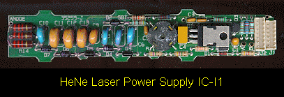
HeNe Laser Power Supply IC-I1 shows the component side of the power supply printed circuit board after the rubbery potting material covering the high voltage section (left half) had been removed. The pot core ferrite transformer is just to the right of center with the IRF630 MOSFET next to it (separated by a filter capacitor). The SG3524 controller IC is located under the IRF630. The bright blue and orange objects are the filter and multiplier capacitors in the high voltage circuitry. The high voltage rectifiers can be seen above and below them. The 99K ohm ballast resistor (3 x 33K) is visible at the far left.
As a result of the sophistication of the SG3524, the overall design is really quite simple. The PWM controller is shown first followed by the inverter:
      2N3904                                     R3
       Q3 +---+-----------------------------+---/\/\---+
          |   | 2.21K                       |  3.92K   |    R5
        |/ C  /    +------------------------|----------+---/\/\---o CS
  VS o--|     \ R1 |      U1 SG3524         |              6.81K
        |\ E  /    |   +--------------+     |
          |   |    |  1|              |16   |   Input (+5 to +12 VDC)
          +---+----|---|-In   Vref Out|-----+         o
          |   |    |  2|              |15             |               1 o  T1
         _|_  / R2 +---|+In        Vin|----+----+-----+-----+------------+
      C3 ---  \ 2.74K 3|              |14  |    |           |         15T )::
     .1uF |   /     ---|Osc Out    E-B|--- |   _|_ C1      _|_ C4     #26 )::
          |   |       4|              |13  |   --- 6.8uF   --- 100uF    2 )::
          +---+----+---|+CL Sense  C-B|--- |    |  16V      |  16V    +--+
                   |  5|              |12  |   _|_         _|_     D  |
                   +---|-CL Sense  C-A|----+    -           -    .|---+ Q1
                   |  6|              |11          D1           G||<--. IRF630
         +---------|---|RT         E-A|---------+--|>|---+-------'|---+
         |         |  7|              |10       | 1N4148 |         S  |
         |     +---|---|CT    Shutdown|---o OV  |        |            |
         |     |   |  8|              |9        |      |/ E Q2        |
      R4 /     |   +---|Gnd       Comp|---      +------|    2N3906    |
    5.1K \    _|_  |   |              |         |      |\ C           |
         /    ---  |   +--------------+         / R6     |            |
         |  C2 |   |                            \ 4.7K   |            |
         |.001 |   |                            /        |            |
         |  uF |   |                            |        |            |
         +-----+---+----------------------------+--------+------------+--o HV-
                  _|_
                   -

      3             C6              C8              C9
 T1 +---------------||------+-------||------+-------||------+
 ::(                        |               |               |
 ::( 250T              D2   |  D3      D4   |  D5      D6   |  D7       HV+
 ::( #43            +--|>|--+--|>|--+--|>|--+--|>|--+--|>|--+--|>|--+----o
 ::(                |               |               |               |
 ::( o 4            |         C7    |               |      C10      |  R14
    +----+----+-----+----+----||----+   +-----+-----+-------||------+--/\/\--+
         |    |     |    |          |   |     |     |                  33K   |
   CS o--+ R7 /  R8 /   _|_ C5      |  _|_   _|_   _|_                   R13 /
          10K \ 430 \   --- .1uF    |  ---   ---   ---                   33K \
          SBT /     /    |          |   | C11 | C12 | C13    LT1             /
              |     |    |          |   |     |     |   +----------+ R12 33K |
  HV- o-------+-----+----+--------------+-----+-----+---|-|       -|---/\/\--+
           R9        R10     R11    |        _|_  Tube- +----------+ Tube+
   OV o---/\/\---+---/\/\----/\/\---+         -
          13K    |   4.7M    4.7M       D2-D7: 2 KV, fast recovery type.
   VS o----------+                      C6-C8, C10: 1nF, C9: 4.7nF, all 3KV.
                                        C11-C13: 1nF, 6KV.
With the installed values for R7 (SBT), the sensitivity is approximately .4 V/mA. The voltage on the +In pin of the SG3524 will then be equal to: 3.24 V - 146 * Iout. The 3.24 V reference is derived from Vref (5 V) and the voltage divider formed by R3, R5, R7, and R8. The factor of 146 comes from the voltage divider formed by R3 and R5 when driven by CS.
              -In = +In
             2.77 = 3.24 - 146 * Iout

   Thus:     Iout = 3.2 mA (for the installed value of SBT).
There is a core gap which is about .005".
Estimated maximum effective V(peak) (since the output is not symmetric, this isn't really precisely defined): 1000 V.
I have estimated the turns ratio for now but intend to perform some measurements to confirm. This is very rough at this point!
The primary appears to be wound first close to the core.
I suspect that like a normal (TV or monitor) flyback transformer, the secondary is built up of several (single thickness) layers of windings (perhaps 40 or 50 turns each) with mylar insulating tape in between.
To somewhat confirm the the turns ratios, I measured the peak-peak input and output of the transformer while operating with a 1 mW HeNe tube: input was 15 V p-p; output was 700 V p-p.
Since this is a flyback converter and the transformer has a core gap, I don't know how closely this correlates with winding ratios but at least it is in the ballpark.
       |                         |           |
    ---+--- are connected;    ---|--- and ------- are NOT connected.
       |                         |           |
These are both based on small flyback transformers and run on low voltage DC. For this, I use a very basic transformer/rectifier/filter capacitor power supply driven from a Variac.
No starting circuit is needed because of the wide compliance of thess circuits. With no load (tube not lit), the voltage will climb to 5 to 8 KV or more. As soon as the tube fires, the output drops to the sustaining ballast resistor voltage for the operating current. In essence, the poor voltage regulation of the inverter represents an advantage and allows this minimalist approach to be effective.
This is one type of design where monitoring of the input voltage to the tube is possible with a VOM or DMM requiring at most a simple high voltage probe. Parasitic voltage multipliers may not have enough current capability and pulse type starting circuits produce short high voltage pulses. It is possible to clearly see the voltage to the ballast resistor/tube ramp up until the tube starts and then settle back to its operating voltage. For small tubes, I can safely use my Simpson 260 VOM on its 5 KV range without a high voltage probe though it may go off scale momentarily.
The only additional components required for the HeNe laser power supplies may be one or two high voltage rectifiers and a high voltage filter capacitor. Since this is across the output at all times, it must be able to withstand the starting voltage but be large enough to minimize ripple when the tube is operating.
CAUTION: I would recommend using higher voltage capacitors than those shown unless you know that your inverter is not capable of reaching the capacitor's breakdown voltage. With some of these on a variable supply, 25 KV or more open-circuit is quite possible due to wiring problems, no tube connected, a bad or high starting voltage tube - or carelessness in turning the knob to far clockwise!
I have also tried a 500 pF, 20 KV doorknob capacitor on design #2 (I didn't have two such caps as required for design #1). While this low value works, it is a bit too small and results in about 20% ripple at an operating voltage of 1,900 V and current of 4 mA with a 15 kHz switching frequency. The minimal tube current setting for stable operation is slightly increased. At lower switching frequencies it will be worse and may prevent the tube from running stably at all. A few of these caps in parallel would be better. Or, use a stack of parallel plate capacitors made from aluminum foil and sheets of 1/8" Plexiglass. :-)
WARNING: Since the voltage rating of these capacitors needs to be larger than for power supply designs with separate starting circuits, it is possible for a nasty charge to be retained especially if the tube should not start for some reason. Stored energy goes up as V*V!
Note: The difference in energy stored in the filter capacitor between the starting and operating voltages is dumped into the tube when it starts. For long tube life this should be minimized. Therefore, a smaller uF value is desirable for these high compliance designs. I do not know how much of an issue this really represents. A post-regulator can be used to remove the larger amount of ripple which results with samller capacitors. However, such a regulator must have overvoltage protection since at the instant the tube fires, it will momentarily see most of the starting voltage.
Thus, it is an extremely simple circuit with no adjustments. Power output is controlled strictly by varying input voltage. Only a pair of high voltage rectifiers and a pair of high voltage filter capacitors for the doubler are required to complete the power supply.
It requires between 6 and 12 VDC (depending on HeNe tube power and ballast resistor) at less than 2 A and will power small HeNe tubes requiring up to about 6 mA at 2,000 V, perhaps more.
Estimated specifications (SG-HI1):
The filter capacitor must be rated for the *maximum* no load voltage possible with your inverter. For testing, I constructed it from two .25 uF, 4,000 V oil filled capacitors in series with equalizing resistors providing about .12 uF at 8 KV. With the components I used, the maximum no load output voltage was slightly less than 8 KV with a 12 VDC input which is more than adequate to start most smaller tubes. However, capacitors with at least a 5 KV breakdown voltage rating (10 KV total) should really be used.
                  +--------------+ X       D3                   Rb
     Vin+ o-------|              |---+-----|>|-----+-----+-----/\/\----+
                  |    Simple    |   |             |     |     100K    |
 8 to 12 VDC, 2 A |   Inverter   |   |         C1 _|_    / R3   5W     |Tube+
                  | Power Supply | T |      .25uF ---    \ 2.2M      .-|-.
     Vin- o-------|              |---|--+  4,000V  |     /           | | |
                  +--------------+   |  |          |     |           |   |
                                     |  +----------+-----+           |   | LT1
                                     |             |     |           |   |
                                     |         C2 _|_    / R4        |   |
                                     |      .25uF ---    \ 2.2M      ||_||
                                     |     4,000V  |     /           '-|-'
                                     |             |     |     R5      |Tube-
                                     +-----|<|-----+-----+----/\/\-----+
                                           D4                  1K     _|_
                                                                       -
The tube current may be monitored as a voltage across R5 (1 V/mA) or directly.
It may be varied by adjusting the input voltage to the inverter. Using a
different ballast resistor value may also help to stabilize operation.
It requires between 8 and 15 VDC (depending on HeNe tube power) at less than 2 A and will power small HeNe tubes requiring up to about 6 mA at 2,500 V, perhaps more. With a 1 mW tube (1,900 V, 4 mA, 150K ballast resistor), the input is about 8 VDC (probably about 1.5 A, not measured) and the switching transistor heat sink doesn't even get warm. :-)
Estimated specifications (SG-HI2):
The high voltage rectifier is built into the flyback transformer. If you have to use an external rectifier, it should be rated at least 20 KV PIV (possibly higher depending on the capabilities of your particular inverter). The filter capacitors shown were just for testing. High voltage types are recommended, again depending on the maximum output of your inverter with no load. For testing, I constructed it from three .25 uF, 4,000 V oil filled capacitors in series with equalizing resistors providing about .08 uF at 12 KV. However, with the design as implemented, the maximum no load output voltage could easily exceed 15 KV with a 15 VDC input.
                     +--------------+ HV+
        Vin+ o-------|              |---------------+-----+-------------+
                     |  Adjustable  |               |     |             |
   8 to 15 VDC, 2 A  | High Voltage |           C1 _|_    / R1          |
                     | Power Supply | HV-    .25uF ---    \ 2.2M        / Rb
        Vin- o-------|              |---+   4,000V  |     /             \ 150K
                     +--------------+   |           |     |             / 5W
                                        |           +-----+             |
                                        |           |     |             |Tube+
                                        |       C2 _|_    / R2        .-|-.
                                        |    .25uF ---    \ 2.2M      | | |
                                        |   4,000V  |     /           |   |
                                        |           |     |           |   |
                                        |           +-----+           |   | LT1
                                        |           |     |           |   |
                                        |       C3 _|_    / R3        |   |
                                        |    .25uF ---    \ 2.2M      ||_||
                                        |   4,000V  |     /           '-|-'
                                        |           |     |      R4     |Tube-
                                        +-----------+-----+-----/\/\----+
                                                                 1K    _|_
                                                                        -
The tube current may be monitored as a voltage across R4 (1 V/mA) or directly.
It may be varied by adjusting the frequency and pulse width controls on the
inverter and its input voltage. Using a different ballast resistor value may
also help to stabilize operation.
It should be possible to add feedback from a current sense resistor to one of the 555 timers to regulate output current by controlling switching frequency or pulse width. This is left as an exercise for the student. :-)
Thus, for small HeNe tubes, this may be all you need. And, you can always use it as the starter when you find some larger ones.
Its wide compliance operation is quite similar to that of the circuit described in the section: Sam's Inverter Driven HeNe Power Supply 2 (SG-HI2) but is somewhat simpler and easier to construct. I do not know how its maximum output power compares but it can be easily scaled up if needed (larger flyback, larger driver transistor, and possibly a beefier DC supply to power it).
This design uses the flyback from a mono computer monitor driven by an NPN darlington power transistor that used to be a solenoid driver from a dead dot matrix printer. By using the high gain darlington rather than a regular deflection or audio power transistor, a 556 timer IC can connect to its base without any matching transformer or additional active components.
The flyback was modified by adding the drive winding on the exposed leg of the core - 20 turns of #24 magnet wire on an insulating sleeve. The high voltage rectifier is built into the flyback.
Frequency and pulse width are adjustable with optimal values for the particular implementation shown in ()s. (See the calculations below.)
Estimated specifications (Kim-I1):
                                                    +12
                                                     o         Flyback
                                                     |        o  T2  +--|>|--o
                                       S1 Start      +---------+ ::(        +
                                R4       _|_  R5 4.7K|          )::(
                        +---+--/\/\---+--- ---/\/\---+    D 20T )::(  Starter
   (7.3K)              _|_  |  1K .1  |       R6 1.5K|      #24 )::(  Output
    10K     1K          -   +---+ uF  |     +--/\/\--+          )::(
    R7      R8   .001uF C2 _|_  | C3  |     | R9 2.2K       +--+ ::( o      -
 --/\/\----/\/\---------+  --- _|_  +-+ +---|--/\/\--+      |        +-------o
    ^                   |   |  ---  |   |   |        |      +--+
    |   +12 o--+----+   +---+   |   |   |   +----+   |         |
    |          |  14| 13| 12| 11| 10|  9|  8|    |   |    +----+------+----+
    +----------+  +-+---+---+---+---+---+---+-+  |   |    |    |C     |    |
    |             | V   Di  Th  Co  Re  O   Tr|  |   | B|/     |      |    |
    |             | c   2   2   2   2   2   2 |  |   +--|      |  C4  | D1 |
    |             | c                         |  |      |\     | .01 _|_  _|_
    |             |    U1 NE556 Dual Timer    |  |        |  |/   uF ---  /_\
    |             |                         G |  |   Q1   +--|        |    |
    |             | 1   1   1   1   1   1   n |  |   2SD1308 |\ E     |    |
    |             | Di  Th  Co  Re  O   Tr  d |  |             |      |    |
    |             +-+---+---+---+---+---+---+-+  |             +------+----+
    v              1|  2|  3|  4|  5|  6|  7|    |            _|_        FR304
 --/\/\--/\/\--+----+   |   |   o   +---|---|----+             -
   R10   R11   |   R12  |   |  +12      |   |
   50K    1K   +--/\/\--+---|-----------+   |  Q1: Darlington from NEC printer
 (13.9K)           330  |   |               |  D1: Damper diode (high speed)
                       _|_ _|_ C6           |
                    C5 --- --- .1uF         |  Note: Additional bypass caps on
              .0033 uF  |   |               |        +12 source recommended
                        +---+---------------+        near the drive input to
                       _|_                           the flyback (not shown).
                        -
C4 and D1 need a voltage rating sufficient for the spike that results when
Q1 turns off. Its magnitude will depend on the inductance of the flyback and
total capacitance (C4 + flyback). The value of C4 is one thing that can be
changed to optimize performance but make sure to monitor the pulse across
Q1 (when it turns off) as you bring up the input voltage and adjust the
frequency and/or pulse width to avoid exceeding the transistor's Vce breakdown
rating. D1 should be a high speed (fast recovery) type.
The only somewhat critical components are C5 and R10+R11 to set the operating frequency, and C2 and R7+R8 to set the pulse width.
In this drawing, frequency is (Timer 1):
                   1.44                          1.44
  F = -------------------------------- = ------------------------ = 28.044 kHz
       ((R10 + R11 + (2 * R12)) * C5)     (14900 + 660) * 3.3E-9
and the pulse width is (Timer 2):
T = (1.1 * (R7 + R8) * C2) = (1.1 * 8300 * 1E-9) = 9.13 uSOptimum frequency and pulse width will depend on the flyback transformer actually used and your needs. I assume the values in (), above, were chosen to maximize output power).
A 12 V, 2 A power supply will likely be needed.
S1 would be a toggle/slide switch or omitted entirely (pin 10 of U1 tied high).
Since the circuit is fired up only rarely, average current requirements are quite low. The +12 V power supply was salvaged from the same monitor as the flyback. It uses a full wave bridge rectifier with a 3,300 uF filter capacitor and is adjustable from around 9.5 V to 13 V. There are separate V+ feeds from the power supply for the 556 and flyback. There are a 100 uF electrolytic, 10 uF tantalum, and a .01 uF disk keeping the 556 happy. A larger main filter capacitor or post filter capacitor may be desirable due to the pulsed nature of the load.
The Start switch, S1, is a momentary pushbutton and enables the drive on demand.
As expected, there is no information on the special ferrite transformer which they (the author of the book) expect you to obtain from Information Unlimited. If it is still available, I expect the cost to be about $10.
See the section: Simple Inverter Type Power Supply for HeNe Laser for details on a similar design that you can build if you are willing to wind your own transformer or use the flyback from a small B/W TV or monochrome computer monitor.
My guess is that this never worked (at least not for more than a few milliseconds) as it depends on putting 110 VAC into the 9 V winding of a little transformer. These are not normally designed with any substantial margins. It probably operates mostly in core saturation likely melting down or blowing up or both in short order. Perhaps (generously) the author was mistaken about the transformer or (more likely) never actually built the thing at all.
I include a reference to it here only to warn that I do not recommend this as a viable option.